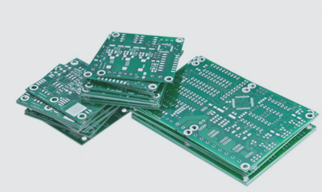
Understanding Multilayer PCB Technology
Exploring the Evolution of PCBs
PCBs have a long history of development, with newer versions constantly emerging. Initially, PCBs reduced in size until reaching a limit. This limitation led to the innovation of multilayer PCBs, enabling the integration of large circuits into compact spaces.
What Sets Multilayer PCBs Apart?
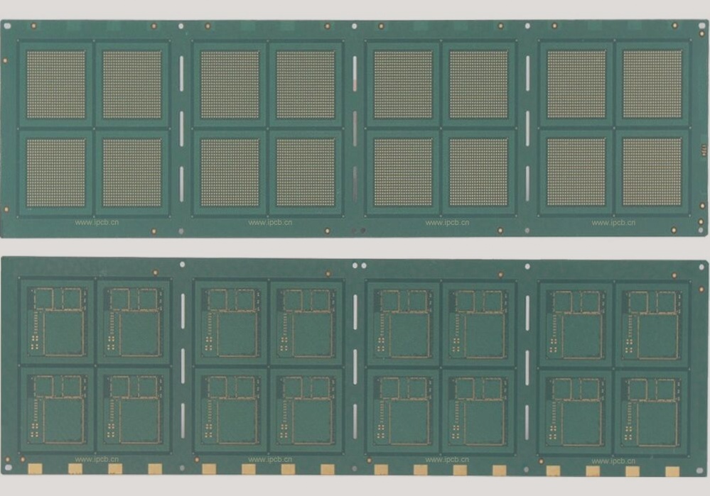
Multilayer PCBs consist of two or more PCB layers stacked together like a sandwich. This advanced technology is commonly found in modern devices like smartphones and tablets.
The Process Behind Multilayer PCB Fabrication
1. Front-end Engineering
The initial step involves designing and engineering the PCB, tailored to its unique functionality. This phase includes meticulous planning, designing, editing, prototyping, and penalization to layout the connection design efficiently.
- Planning
- Designing
- Editing
- Prototyping
- Penalization
After several iterations, the optimal PCB prototype is developed for subsequent processes.
2. Photo Plotting
Utilizing a laser photoplotter, this stage involves plotting images directly onto the dry film of the PCB. This enhances accuracy, reduces manufacturing time, and cuts down costs, with variations in the process for different layers.
3. Imaging, Developing, Etching, and Stripping
This phase includes creating traces, pads, and metal grounds on the PCB through imaging and developing. Subsequently, etching and stripping prepare the PCB surface for copper plating by following a specific pattern, resulting in conductive copper patterns for the inner layers.
4. Automated Optical Inspection
To ensure accuracy, the PCB undergoes automated optical inspection, where images are compared against provided data to identify any discrepancies like missing connections or etching issues, preventing problems in subsequent processes.
5. Oxide Chemical Treatment
This step enhances the roughness of copper contact pads, facilitating better bonding between layers and ensuring a robust multilayer PCB structure.
6. Lamination
Through lamination, the conductive and nonconductive parts of the PCB are fused using high temperature, pressure, and a hydraulic press, melting and bonding the layers together effectively.
7. Drilling for Required Holes
PCB Manufacturing Process Overview
Drilling for Component Placement
Drilling plays a crucial role in PCB manufacturing as components may need to pass through holes before being soldered. These holes are essential for mounting the PCB within the device.
Copper Deposition for Conductivity
To make the PCB conductive, a thin layer of copper is deposited on the exposed layers, including the freshly drilled holes. This is achieved through a special electroplating process.
Photoresist Layer Application for Electroplating
Preparing the PCB for electroplating involves applying a photoresist outer layer using laminator machines and direct imaging techniques. This creates a conductive pattern for the copper plating process.
Electroplating for Copper Layer
The PCB undergoes electroplating to plate copper onto the conductive pattern, ensuring a simplified process. Additionally, a tin plating bath is used to protect the copper patterns during etching and stripping.
Stripping and Etching for Circuit Completion
Through the SES process, the PCB is stripped to expose the copper patterns and remove excess copper. This step finalizes the electrical circuit-making process in preparation for soldering.
Solder Masking for Circuit Protection
Solder masking prevents short circuits by applying an epoxy-based resist on the PCB surface. The screen printing process covers the panel entirely, and UV light cures the layer to protect the copper patterns.
Surface Finish Application for Heat Protection
To safeguard against heat during soldering, a surface finish is applied to cover exposed copper sections and prevent oxidation. This ensures the PCB remains safe from heat and oxidation.
Automated Circuit Testing for Quality Assurance
Before finalizing the PCB, automated circuit testing is conducted to ensure the circuits are defect-free. Flying probe testers verify that all circuitry meets the required standards without any issues.
Fabrication and Inspection for Finalization
Once the PCBs are shaped and separated from the panel using CNC machines, each individual PCB undergoes inspection to ensure it meets visual and performance standards. Inspectors review documentation and physically check the PCB for quality assurance.
Understanding Multilayer PCB Manufacturing Process
Ensuring that each unit meets the exact specifications of the customer is a crucial step in the multilaminate PCB manufacturing process. Once this thorough inspection is completed, the manufacturing process for multilayer PCBs comes to a close.
The Complexity of Multilayer PCB Manufacturing
While multilayer PCB manufacturing may appear straightforward, it involves intricate steps that differentiate it from the production of simple PCBs. These unique processes, although slightly different or supplementary, are essential in achieving the marvels of technological progress and innovation. By familiarizing yourself with the multilayer PCB manufacturing process, you gain insight into the intricacies of this advanced technology.