Understanding PCB Fabrication and Assembly Process
PCB fabrication is a crucial procedure in producing simple boards that serve as the foundation for printed circuit board assembly. Careful consideration is essential when selecting a PCB fabrication service to avoid potential damages that could render the product useless. Effective communication between the design team and manufacturers is key to a successful outcome.
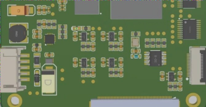
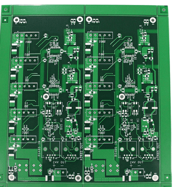
It’s important to note that PCB fabrication and assembly are distinct stages in the PCB engineering process. Fabrication involves translating a circuit board design onto an existing board structure, while assembly entails physically placing components on the board to enable its functionality.
Key Differences Between PCB Fabrication and Assembly
- Fabrication focuses on producing the actual printed circuit board.
- Assembly involves the attachment of components to the board.
Step-by-Step PCB Fabrication Process
Let’s delve into the sequential steps of the PCB fabrication process:
- Direct Laser Imaging and Progress Process
Prior to commencing work on a PCB design, direct laser imaging is utilized to target areas that will form the metal base of the design. A dry film is applied to a copper plate, and laser imaging exposes specific areas, leaving them as barriers. The film is then removed, leaving behind the copper circuits.
- Bonding through Lamination and Oxidation
Following the prominent layering, a chemical treatment involving oxidation is applied to enhance the board’s strength. This process reinforces the integrity of the printed circuit board.
PCB Fabrication Process
During PCB fabrication, several crucial steps are involved to ensure the proper functioning of the circuit board.
Drilling and Hole Alignment
- Drilling precise holes according to component requirements is essential.
To enable signal transmission between layers, holes are drilled or lasered with meticulous alignment.
The depth and alignment of these holes are critical for successful PCB functionality.
Copper Deposition and Outer Layer Coating
- Ensuring Copper Deposition and Coating
After drilling, excess debris is cleared, and a copper coating is applied to create a metallic base for further processing.
Outer layers are coated with dry film and imprinted using laser direct imaging for precise design.

Silver-Plating and Surface Finishing
- Applying Silver-Plating and Surface Finishing
Conductive patterns lead to exposed drilled holes, which are then electroplated with copper for conductivity.
Subsequent tin plating forms a protective barrier on the board surface.
Once the plating process is complete, excess materials are chemically removed, leaving copper in specific areas.
At this stage, the printed circuit board is assembled but not yet operational.
Fuse Mask Application and Surface Finalization
Prior to PCB assembly, a fuse mask is applied to protect the board and prevent accidental connections.
The fuse mask, typically green, safeguards copper traces from corrosion.
- Preventing Fuse Bridges and Color Selection
- Choosing the Right Fuse Mask Color
While the fuse mask color choice does not affect PCB functionality, darker colors may not be suitable for high-temperature applications.
Important Steps in PCB Fabrication Process
After applying the fuse mask, orientation designs and board markings are enforced on the printed circuit board. The final step involves finishing the metal surface that is uncovered by using a repair mask.
Testing and Examination
- Final examination and testing are crucial to detect hardware faults.
As the PCB fabrication process nears completion, extensive testing and reviews are conducted to ensure the boards’ functionality is up to standard. This step is essential before assembly or shipping.
The inspection equipment identifies short circuits that could affect the board’s performance, emphasizing the need for thorough testing.
Factors to Consider When Choosing a PCB Fabrication Company
Printed circuit board fabrication is a meticulous process where even a minor error can lead to significant losses if the board construction is flawed.
When selecting a PCB fabrication company, consider their track record of success and achievements. Key factors to evaluate include:
- Excellent customer service and guidance
- Adherence to timelines and effective communication
- Comprehensive testing procedures
- Collaborative approach
- High-quality printed circuit boards
- Utilization of premium materials
Conclusion
PCB manufacturing is a intricate process that begins with product conceptualization and culminates in a fully functional PCB assembly. Attention to detail throughout the fabrication process is crucial for success. Therefore, understanding the intricacies of PCB fabrication is paramount.