**Why do I need to have test points on the PCB?**
Some may wonder: “In PCB circuit board design, why are test points necessary?” This question can be a bit confusing. I recall when I first started as a process engineer at a PCBA manufacturing facility; I sought insights from various colleagues regarding test points to deepen my understanding. Essentially, the primary purpose of incorporating test points is to verify whether the components on the circuit board conform to specifications and exhibit good solderability. For instance, if you want to check for issues with a resistor on a circuit board, the simplest method is to use a multimeter to measure across its terminals. This allows you to easily assess the situation. The details are as follows:
PCB circuit board design: Why do we need test points on the PCB?
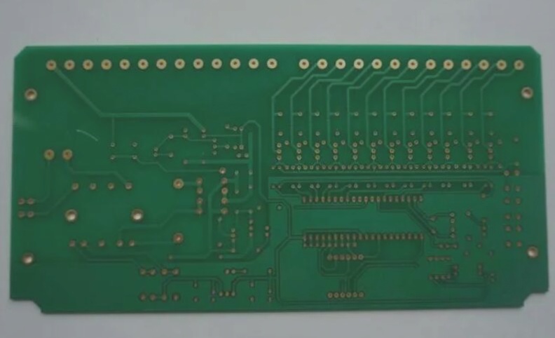
1. However, in mass production environments, it is impractical to use an electricity meter to slowly measure whether each resistance, capacitance, inductance, and even IC circuit on each board is correct. This led to the development of ICT (In-Circuit Test) automated testing machines, which utilize multiple probes (commonly referred to as “Bed-Of-Nails” fixtures) to simultaneously contact all components on the board that require measurement. The characteristics of these electronic components are then assessed sequentially through program control, employing both primary and side-by-side methods. Typically, testing all components on an average board takes about 1 to 2 minutes, depending on the number of parts present; more components generally result in longer testing times.
2. However, if these probes directly touch the electronic components or their solder pads on the board, there is a risk of damaging some parts, which can be counterproductive. To address this, innovative engineers introduced “test points” located at both ends of the components. These are small circular pads without a solder mask, allowing the test probes to contact these pads instead of the actual electronic parts being measured.
3. In the early days of PCB design, traditional through-hole components (DIP) were used, and we often relied on the solder pads of these components as test points. Since the solder pads of traditional components were robust, they could withstand probe contact without concern. However, frequent issues arose with misjudgments due to poor contact. After electronic components underwent wave soldering or SMT assembly, a residue of solder paste flux typically formed on the solder surface, resulting in high resistance and often leading to probe contact issues. Consequently, test operators on production lines were often seen using air spray guns or alcohol to clean the testing areas.
4. In fact, even the test points after wave soldering experienced poor probe contact issues. However, with the rise of SMT, misjudgments in testing were significantly reduced, and the importance of test points became more pronounced, especially since SMT components are typically fragile and cannot tolerate direct probe pressure. Utilizing test points eliminated the need for probes to directly contact the components and their solder pads, which not only protects the components from damage but also greatly enhances test reliability by reducing the likelihood of misjudgments.
5. Nonetheless, as technology has progressed, PCB sizes have become increasingly compact, making it challenging to fit numerous electronic components onto a small circuit board. Consequently, the issue of test points occupying PCB space often leads to a tug-of-war between design and manufacturing teams, a topic that will be addressed further in future discussions. Test points typically appear as circles, as probes are also round, making them easier to manufacture and allowing for closer placement of adjacent probes, thereby increasing the density of the probe bed.
6. The use of a probe bed for circuit testing has inherent mechanical limitations. For instance, there is a minimum diameter limit for probes; those with too small a diameter are prone to breakage and damage. Additionally, the spacing between probes is constrained because each probe must exit a dedicated hole, and the back end of each probe needs to be soldered to a flat cable. If the adjacent holes are too small, not only does this create the risk of contact short circuits, but interference from the flat cables also poses significant challenges.
7. Probes cannot be placed next to taller components. If a probe is positioned too close to a high component, there is a risk of collision that could lead to damage. Furthermore, to avoid interference from taller components, holes must be created in the test fixture’s probe bed, which inadvertently limits the placement of probes. This challenge makes it increasingly difficult to accommodate test points for all components on a PCB.
If you have any PCB manufacturing needs, please do not hesitate to contact me.Contact me

