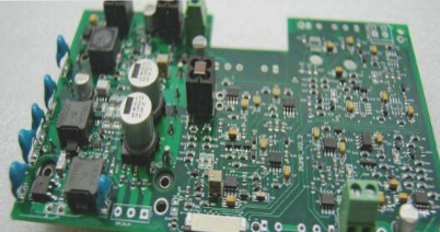
Importance of Test Points in PCB Circuit Board Design
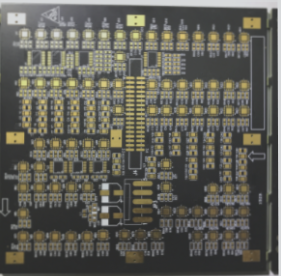
Test points play a crucial role in PCB circuit board design by allowing engineers to verify the functionality and solderability of components. When testing components like resistors, capacitors, and IC circuits, test points provide a safe and efficient way to make contact without risking damage.
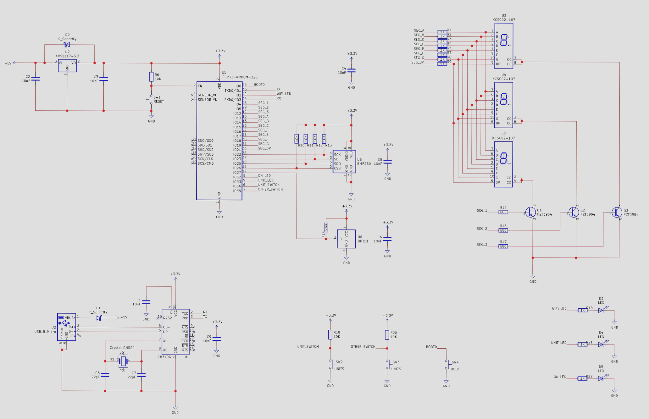
Automated Testing with ICT Machines
In large-scale production environments, manual testing of every component is impractical. Automated test equipment, such as In-Circuit Test (ICT) machines, use “Bed-Of-Nails” fixtures to simultaneously measure designated points on the board. This automated process ensures accurate testing of components under program control.
Evolution of Test Points
In the past, traditional through-hole components served as test points, but issues like poor contact led to the development of dedicated test points. With the rise of Surface Mount Technology (SMT), fragile components required protection from direct probe contact, making test points even more essential for reliable testing.
Challenges and Innovations
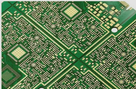
As technology advances and PCBs become smaller, the placement of test points can pose challenges for design and manufacturing teams. The round shape of test points facilitates probe contact and allows for higher probe density in the bed of nails. However, mechanical limitations, such as probe diameter and spacing constraints, must be considered to avoid issues like breakage and short circuits.
- Test points ensure accurate verification of components on PCBs
- Automated ICT machines streamline the testing process in production environments
- Evolution from through-hole components to dedicated test points for SMT components
- Challenges in test point placement and innovations to overcome mechanical limitations
Challenges and Innovations in PCB Testing
- Proximity to Tall Components
- Reducing Test Points
- ICT Needle Implantation
- Importance of Test Points
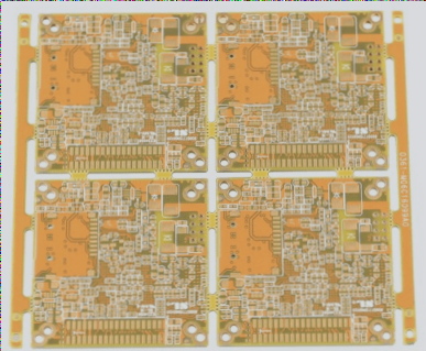
Placing probes near tall components poses a risk of collision, potentially damaging both the probe and the component. Customizing the test fixture needle bed with holes to avoid high parts further limits test point placement, especially as circuit board sizes decrease.
With shrinking circuit boards, the debate over the number of test points intensifies. Methods like Net Test, Test Jet, Boundary Scan, and JTAG aim to decrease test points. Alternative techniques such as AOI and X-ray inspection are also being explored, but no single method can fully replace ICT testing.
Consulting with fixture manufacturers is crucial to understand the minimum test point diameter and spacing between adjacent points. Manufacturers provide desired and achievable minimum values, but large-scale manufacturers may impose additional constraints to prevent test fixture damage.
Test points play a vital role in PCB layout for reliable testing. Understanding their significance and the challenges they present is key to successful PCB testing.
If you have any questions about PCB testing, feel free to reach out to us at info@wellcircuits.com.