1. In the PCB manufacturing industry, when discussing the differences among hard gold, soft gold, and flash gold on circuit boards, insights gathered from years of collaboration with circuit board manufacturers inform the following personal opinions and experiences. Please feel free to correct any inaccuracies.
2. Many colleagues working in PCBA assembly plants often find the distinctions between “hard gold,” “soft gold,” and “flash gold” on circuit boards unclear. Some even believe that electroplated gold must inherently be hard gold, while chemical gold is synonymous with soft gold. In reality, this classification is only partially accurate.
3. The distinction between “hard gold” and “soft gold” in the PCB industry pertains to the concepts of “alloy” versus “pure gold.” Pure gold is inherently softer, while alloys that incorporate other metals are harder and more resistant to wear. Thus, the higher the purity of the gold, the softer it becomes.
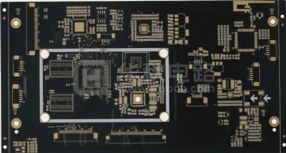
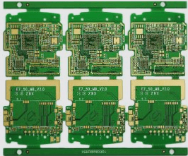
4. Electroplated nickel gold is a key component in this discussion. Notably, “electroplated gold” can indeed be categorized into hard gold and soft gold. Electroplated hard gold is essentially an alloy (composed of gold and other metals), which gives it a relatively high hardness, making it suitable for applications that require durability and resistance to friction. In the electronics sector, it is commonly used for the edges of circuit boards at contact points, known as “gold fingers,” as illustrated in the accompanying image.
5. Conversely, soft gold is typically utilized for aluminum wire connections on COB (Chip On Board) assemblies or for the contact surfaces of mobile phone buttons. Recently, it has seen increased application on both the front and back of BGA substrates.
To understand the origins of hard gold and soft gold, it is helpful to first grasp the process of gold electroplating. Setting aside the initial pickling stage, the main goal of electroplating is to deposit “gold” onto the copper surface of the circuit board. However, if “gold” and “copper” come into direct contact, there will be a physical reaction involving electron migration and diffusion. Therefore, it is essential to first electroplate a layer of “nickel” as a barrier, followed by gold on top of the nickel. Consequently, what we commonly refer to as electroplated gold is more accurately termed “electroplated nickel gold.”
The distinction between hard gold and soft gold lies in the composition of the final layer of gold that is plated. When plating gold, you can opt for pure gold or an alloy. Since pure gold is relatively soft, it is known as “soft gold.” This is particularly relevant in applications involving aluminum wires, as “gold” forms a good alloy with “aluminum,” leading to specific thickness requirements for pure gold in COB manufacturing.
On the other hand, if you choose to electroplate a gold-nickel alloy or a gold-plated alloy, the resulting alloy will be harder than pure gold, which is why it is referred to as “hard gold.”
The electroplating procedures for soft gold and hard gold are as follows:
Soft gold: pickling – electroplating nickel – electroplating pure gold
Hard gold: pickling – nickel plating – pre-gold plating (flash gold) – plating gold-nickel or gold alloy
**Chemical Gold**
Currently, the term “chemical gold” mainly refers to the ENIG (Electroless Nickel Immersion Gold) surface treatment method. Its advantage lies in the ability to adhere “nickel” and “gold” to the copper surface without the complex electroplating process, resulting in a flatter surface than that produced by electroplated gold. This is particularly beneficial for shrinking electronic components that require high flatness and fine pitch.
Because ENIG utilizes a chemical replacement method to create the surface gold layer, its maximum gold thickness generally cannot match that of electroplated gold. Furthermore, the more substantial the underlying layer, the lower the gold content will be.
Due to the replacement principle, the gold layer in ENIG is considered “pure gold,” which is often classified as a form of “soft gold.” Some use it as a surface treatment for COB aluminum wires, although it is critical that the gold layer thickness be at least 3 to 5 micro-inches (μ”). Typically, achieving a gold thickness exceeding 5 μ” is challenging. A too-thin gold layer can compromise the adhesion of the aluminum wire. In contrast, standard electroplated gold can easily reach thicknesses of 15 micro-inches (μ”) or more, although the cost increases with gold layer thickness.
**Flash Gold**
The term “flash gold” derives from the English word “flash,” indicating rapid gold plating. It actually refers to the “pre-gold plating” step in hard gold electroplating. This process initially forms a denser but thinner gold-plated layer on the nickel layer, facilitating the subsequent electroplating of gold-nickel or gold-plated alloys. Some believe that PCBs can be produced in this way, resulting in lower costs and reduced time, which has led to the marketing of “flash gold” PCBs.
Because “flash gold” lacks the subsequent gold electroplating process, its cost is significantly lower than that of true electroplated gold. However, due to the thinness of the “gold” layer, it often fails to adequately cover the underlying nickel layer. Consequently, this can lead to oxidation of the circuit board after prolonged storage, adversely affecting solderability.
Considering the various current PCB surface treatment methods, the cost of electroplating nickel gold is relatively high compared to alternatives like ENIG and OSP. With gold prices soaring, its use has become rare unless for specific applications, such as contact surface treatments for connectors or sliding contact elements (e.g., gold fingers). Nevertheless, regarding current circuit board surface treatment technologies, the electroplated nickel-gold coating remains unmatched in terms of excellent anti-friction and anti-oxidation properties.

