What Does Copper Weight Mean?
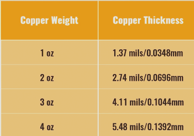
Copper weight refers to the amount of copper applied to each square foot of the PCB surface, typically measured in ounces per square foot (oz/ft²). However, another term commonly encountered is copper thickness. How are copper weight and thickness related? Copper thickness is defined as the measurement of the copper foil’s thickness when a specific weight of copper is spread over 1 square foot. For instance, if 1 oz. of copper is rolled out to cover an area of 1 square foot, the resulting foil thickness will be 1.37 mils or 0.0348 mm.
Below is a chart that illustrates the relationship between copper weight (in ounces) and copper thickness.

Choosing the Right Copper Weight
When selecting copper weight, factors such as trace width, signal integrity, and voltage drop must be considered. For example, if your design needs to handle a high current, a thicker copper weight is necessary to prevent traces from overheating. On the other hand, for maintaining high signal integrity, a thinner copper weight is preferred to reduce the inductance of the traces. PCBs with copper weights exceeding 3 oz, and approaching 4 oz or more, are typically classified as “heavy copper.” Due to their thicker copper layers, heavy copper PCBs are specifically designed to handle higher current loads and offer enhanced thermal management.
Design Considerations for Heavy Copper
Increased Minimum Track Spacing: As the copper weight increases on a PCB, the required spacing between copper features also increases. It is crucial to adhere to the minimum track spacing requirements for different copper weights to prevent issues like signal degradation and overheating. For example, at Wellcircuits, the minimum track spacing for 3 oz copper is 10 mil, for 4 oz copper is 13 mil, and for 5 oz copper is 18 mil.
Increased Via Size: Heavy copper designs are often used in circuits that carry higher currents, making it essential to ensure the vias are capable of handling the required current without excessive resistive losses. Larger vias provide lower impedance paths for current flow, which reduces resistive heating and minimizes voltage drops. This design choice ensures that vias can effectively manage the higher current loads in heavy copper PCBs, ensuring reliable connections between different layers of the board.
Increased Solder Mask Thickness: Due to the higher surface tension of heavy copper, the solder mask may struggle to adhere properly to the copper surface. If the solder mask does not adhere well, it can peel away, exposing the copper traces. This can lead to issues such as shorts, corrosion, and other problems. Increasing the solder mask thickness helps by providing more surface area for the solder mask molecules to bond to, improving adhesion and reducing the risk of failure.
If you have any questions about PCBs or PCBA, please feel free to contact us at info@wellcircuits.com


