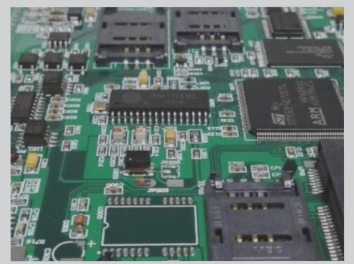
Challenges and Solutions in PCB Design
In recent years, PCB design engineers have faced increasing challenges due to the complexity of products, rapid technological advancements, and tight time-to-market deadlines. Integrating advanced technologies while balancing cost efficiency and functionality is a primary concern. The key lies in applying these technologies effectively to add value without exceeding budget constraints.
Time-to-market is a crucial factor influencing PCB design decisions. Shortening product development cycles require quick decisions and adaptation to changing specifications, leading to difficulties in balancing considerations like product functionality, design implementation, testing, and EMI requirements. Early evaluation and simulation can help identify potential issues before they escalate.
Mentor’s PCB evaluation software offers tools for design validation, assisting engineers in assessing electrical functionality, signal integrity, and EMI compliance. By leveraging such tools, engineers can optimize designs early, reducing the likelihood of encountering significant issues later in development.
Efficiently integrating advanced technologies, meeting time-to-market demands, and minimizing rework is vital for successful PCB design. With the right tools and strategies, engineers can navigate challenges and create high-quality, cost-effective designs that meet industry demands.

Evaluating PCB Design Tools: Key Considerations for Designers
While selecting PCB design tools, designers often face challenges due to budget constraints. Understanding the key factors when evaluating PCB design software is essential to make informed decisions.
Key Factors to Consider When Choosing PCB Design Software:
-
Core Functionality
- Schematic and Layout Integration: Seamless support for interaction between schematic diagrams and PCB layout to ensure data consistency and reduce errors.
- Routing Features: Automatic routing features like fan-out wiring and push-pull routing streamline the design process. Design-rule-based routing ensures compliance with manufacturing specifications.
- Design Rule Checking (DRC): A reliable DRC checker is crucial for error detection and resolution early in the design process.
-
Scalability and Advanced Design Capabilities
As companies move towards complex PCB designs, the software should expand its functionality to meet advanced design requirements.
HDI (High Density Interconnect)
As technology advances, managing HDI interfaces is crucial for denser designs. Utilizing advanced routing techniques and automated script generation tools can help streamline the process.
Flexible Design Options
A good PCB design tool should offer flexible design layouts, allowing for the integration of passive components and high-speed RF designs. This flexibility is essential for adapting to various project requirements.
Comprehensive Simulation Capabilities
Look for a PCB design tool with comprehensive simulation features, including analog, digital, mixed-signal, high-speed, and RF simulations. These capabilities are vital for testing circuit behavior and ensuring design integrity.
Component Library Management
Efficient design relies on easy access to an up-to-date component library. Seek a tool with a centralized library and custom component creation options for specialized designs. This ensures quick access to necessary components without delays.
Partnership and Vendor Support
Choose a software vendor with technical expertise and a commitment to continuous improvement. Strong vendor support is crucial for complex designs, reducing downtime, and ensuring successful project outcomes.
Cost Considerations: Return on Investment
While cost is a factor, prioritize the return on investment when selecting a PCB design tool. Balance upfront costs with long-term productivity gains to avoid limitations in functionality that may impact design quality and time-to-market.
Balancing Design Flexibility and Constraints
Modern designs require a balance between design flexibility and constraints. Define critical design paths and constraints while allowing for design freedom when necessary. Understanding design requirements is key to achieving successful outcomes.
Synchronization Between Design and Layout
Ensuring synchronization between design and layout stages is crucial for a smooth PCB design process. Integrated design constraints and rules across both stages minimize errors and inconsistencies, leading to more efficient and accurate designs.
By considering these factors, PCB designers can choose tools that meet their needs and support efficient, innovative design processes. Selecting a tool that can scale with the complexity of future projects is essential for staying competitive in the ever-evolving PCB industry.