Hello guys,
I know that a lot of PCB manufacturers remove unused (not connected) via pads’s to reduce drill bit tear:
My CAD package (Altium) has an option to do this when generating Gerbers or in Altium itself when routing is (almost) done.
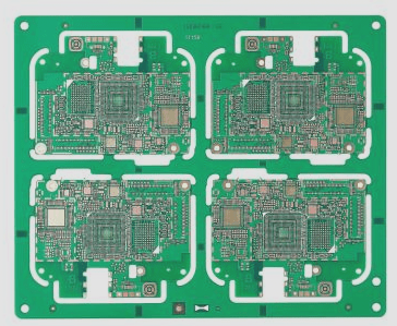
When I do this in the Gerber output I end up with copper the same as in my CAD package but with the unused via pads removed (see image 1). This is how a manufacturer would do this.
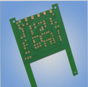
But, when I order Altium to do this and repour my planes/polygons I end up with much more copper because it uses my clearance rule (100um) as a distance between the via barrel and the copper. (image 2). This is nice because this way I have much more copper on my planes = lower inductance = better SI and PI.
But I assume (that is where u guys come in) using the normal 100um clearance between the via barrel and the copper is not enough clearance for the via plating process or is it?
So, what would be a reasonable clearance between an (plated) via hole with no pad on the particular layer and other copper on that layer?


