Understanding the Significance of Solder Paste Inspection
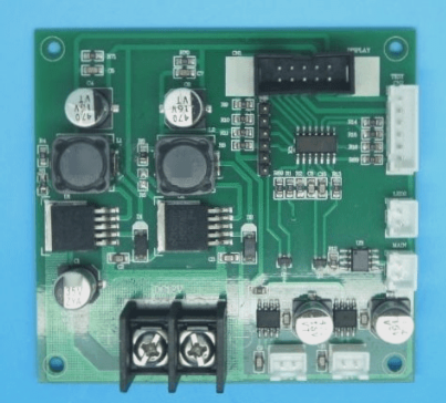
Solder Paste Inspection (SPI) is a crucial technical procedure used to analyze solder paste deposits on a Printed Circuit Board (PCB) during the manufacturing process. This inspection helps identify defects such as solder percentage variations, missing solder, and other issues.
SPI plays a vital role in ensuring the correct deposition of solder on the PCB. Detecting and rectifying solder joint issues early on can significantly reduce rework and costs associated with soldering processes.
Exploring Solder Paste and its Role
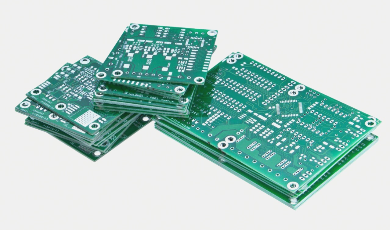
Solder paste consists of fine metal solder grains mixed with flux, creating a paste-like consistency. The composition of flux and the size of metal particles determine the characteristics of the solder paste. Different types of solder paste, such as no-clean solder paste and rosin-based solder paste, are used in PCB assembly processes.
In PCB assembly, solder paste is applied to attach components to the board. Upon heating in an infra-red reflow device, the solder paste melts and forms strong soldered joints, securing the components in place.
Techniques for Printed Circuit Board (PCB) Solder Paste Inspection
Two main techniques are commonly used for SPI on printed circuit boards:
- Automated Optical Inspection (AOI):
AOI machines are equipped to detect various defects on PCBs, including surface defects, component placement errors, and dimensional inaccuracies. By capturing images, AOI systems can identify missing components, incorrect placements, and other issues, ensuring high-quality PCB assembly.
- Automated X-Ray Inspection (AXI):
AXI utilizes X-ray radiation to inspect solder paste quality on PCBs. Unlike AOI, AXI provides greyscale images that help identify defects like thermal issues, BGA defects, and solder gaps. This non-destructive testing method offers a deeper analysis of PCB solder joints.
The Role of AOI and AXI in Solder Paste Inspection
Both AOI and AXI techniques play crucial roles in solder paste inspection for identifying errors and preventing defects in PCBs, ultimately saving costs.
Understanding Solder Paste Inspection Process
Solder paste inspection (SPI) involves capturing the PCB image and comparing it with the expected model through template, pattern, and statistical analysis methods.
- Template matching compares the actual image with the expected one, while pattern and statistical comparisons analyze different aspects of the board.
- Some SPI processes utilize a specialized camera for video streaming, known for its high-speed capabilities.
- Proper lighting, including fluorescent, LED, or infrared, is crucial for efficient defect identification. Correct positioning of the lighting source highlights every detail on the board, ensuring no component is overlooked.
Significance of Solder Paste Inspection
Thorough solder paste inspection ensures error-free and durable PCBs, enhancing overall infrastructure and performance.
- High-quality appliances and angled cameras enable the capture of detailed 3D images, improving fault detection and component examination.
- Identifying paste quantity discrepancies can prevent long-term PCB damage, saving costs and enhancing product longevity.
Final Thoughts on Solder Paste Inspection
For flawless, high-quality PCBs, solder paste inspection is indispensable. It not only eliminates defects but also prevents future damages, ultimately reducing delivery time and additional expenses for manufacturers.