1. PCB assembly preparation primarily involves the creation of various process documents essential for circuit assembly.
2. This process encompasses product documentation and operational documents necessary for organizing production.
3. The product documentation is further categorized into two types: one type is based on projection diagrams, which detail product processing and assembly requirements, parts, and printed circuit board assembly drawings.
4. The other type utilizes graphical symbols to convey the design content of the circuit, including system diagrams, block diagrams, circuit diagrams, wiring diagrams, and more.
5. A block diagram serves as an annotated representation that outlines the fundamental components, interrelationships, and key characteristics of electronic products.
6. In the block diagram, each “box” signifies a functional block, while each “line” illustrates the signal path or sequence through the circuit.

2. Circuit Diagram
A circuit schematic diagram, also known as an electrical schematic diagram or electronic circuit diagram, illustrates the arrangement of various components within a product. This diagram does not consider the actual locations of the components nor their shapes and sizes. It is based on the circuit block diagram and serves as the foundation for design, wiring, product performance analysis, and maintenance.
Creating the circuit schematic requires an accurate, aesthetically pleasing, and logical layout. Typically, the input signal is placed on the left, and the output signal on the right, with component symbols adhering to the drawing standards. Identical component symbols are numbered sequentially from left to right or top to bottom. Wires connecting components are depicted as lines, and junctions of two or more wires are indicated with solid dots, signifying that the wires cross but do not connect. In the circuit diagram, the “floor” is represented by the symbol “X,” and all grounds must be interconnected by wires.
3. List of Supporting Materials
The supporting material list catalogs the names and specifications of materials needed for electronic products, including quantities for procurement and assembly, along with a table of equipment codes.
4. Schematic Diagram of Parts
The component schematic diagram encompasses both the printed circuit board (PCB) assembly diagram and the chassis panel schematic.
(1) Printed Circuit Board Assembly Drawing
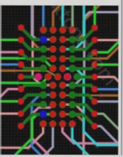
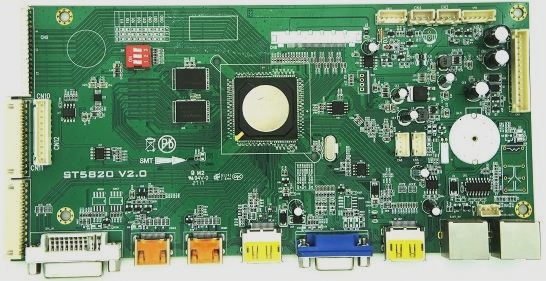
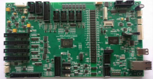
The PCB assembly drawing visually represents the connection relationships between components and the PCB. It is essential for the assembly and soldering processes of PCBs. This drawing bridges the schematic circuit diagram and the actual circuit board, serving as a critical reference during electronic assembly and maintenance, and is often utilized for testing and locating components.
(2) Schematic Diagram of the Chassis Panel
The chassis panel schematic diagram outlines the installation of various components within the chassis. For simpler products like superheterodyne radios, a chassis panel schematic is typically unnecessary. However, for more complex electronic products, additional process documents may include wiring diagrams and tables, which are not detailed here.
5. Wiring
For straightforward electronic PCB products, wiring may not be necessary. However, in complex products with numerous connections, the wiring can become intricate, making it challenging to locate components or affecting the overall appearance. Therefore, it is generally required to draw and tie wires for clarity.
6. Assembly Drawing of the Whole Machine
The assembly drawing of the entire machine indicates the assembly positions and overall appearance of the components.
2. This process encompasses product documentation and operational documents necessary for organizing production.
3. The product documentation is further categorized into two types: one type is based on projection diagrams, which detail product processing and assembly requirements, parts, and printed circuit board assembly drawings.
4. The other type utilizes graphical symbols to convey the design content of the circuit, including system diagrams, block diagrams, circuit diagrams, wiring diagrams, and more.
5. A block diagram serves as an annotated representation that outlines the fundamental components, interrelationships, and key characteristics of electronic products.
6. In the block diagram, each “box” signifies a functional block, while each “line” illustrates the signal path or sequence through the circuit.
2. Circuit Diagram
A circuit schematic diagram, also known as an electrical schematic diagram or electronic circuit diagram, illustrates the arrangement of various components within a product. This diagram does not consider the actual locations of the components nor their shapes and sizes. It is based on the circuit block diagram and serves as the foundation for design, wiring, product performance analysis, and maintenance.
Creating the circuit schematic requires an accurate, aesthetically pleasing, and logical layout. Typically, the input signal is placed on the left, and the output signal on the right, with component symbols adhering to the drawing standards. Identical component symbols are numbered sequentially from left to right or top to bottom. Wires connecting components are depicted as lines, and junctions of two or more wires are indicated with solid dots, signifying that the wires cross but do not connect. In the circuit diagram, the “floor” is represented by the symbol “X,” and all grounds must be interconnected by wires.
3. List of Supporting Materials
The supporting material list catalogs the names and specifications of materials needed for electronic products, including quantities for procurement and assembly, along with a table of equipment codes.
4. Schematic Diagram of Parts
The component schematic diagram encompasses both the printed circuit board (PCB) assembly diagram and the chassis panel schematic.
(1) Printed Circuit Board Assembly Drawing
The PCB assembly drawing visually represents the connection relationships between components and the PCB. It is essential for the assembly and soldering processes of PCBs. This drawing bridges the schematic circuit diagram and the actual circuit board, serving as a critical reference during electronic assembly and maintenance, and is often utilized for testing and locating components.
(2) Schematic Diagram of the Chassis Panel
The chassis panel schematic diagram outlines the installation of various components within the chassis. For simpler products like superheterodyne radios, a chassis panel schematic is typically unnecessary. However, for more complex electronic products, additional process documents may include wiring diagrams and tables, which are not detailed here.
5. Wiring
For straightforward electronic PCB products, wiring may not be necessary. However, in complex products with numerous connections, the wiring can become intricate, making it challenging to locate components or affecting the overall appearance. Therefore, it is generally required to draw and tie wires for clarity.
6. Assembly Drawing of the Whole Machine
The assembly drawing of the entire machine indicates the assembly positions and overall appearance of the components.