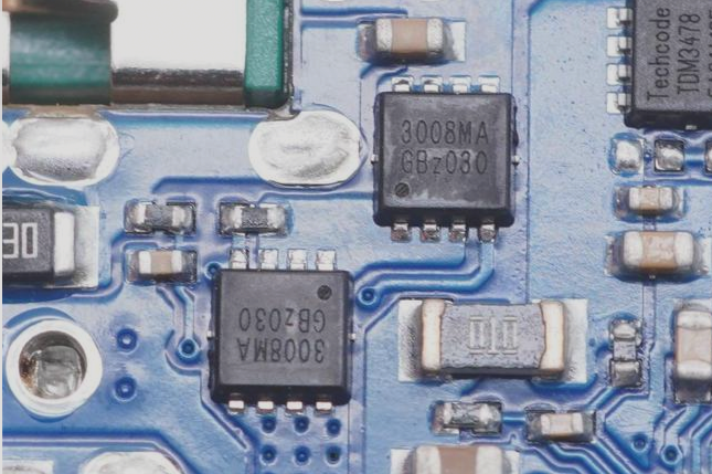
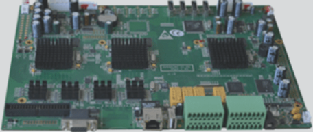
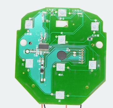
2. Commonly used copper laminates include copper phenolic paper laminates, copper epoxy paper laminates, copper epoxy glass cloth laminates, copper epoxy phenolic glass cloth laminates, copper PTFE glass cloth laminates, and epoxy glass cloth multilayer printed circuit boards.
3. Each laminate material has unique characteristics. Epoxy resin and copper foil exhibit excellent adhesion, offering high bond strength and resistance to high temperatures. As a result, copper foil can withstand molten tin at 260°C without degrading.
4. Glass cloth laminates impregnated with epoxy resin are more resistant to humidity compared to other types. For UHF (Ultra High Frequency) circuit boards, copper PTFE glass cloth laminates are often the preferred choice due to their superior performance at higher frequencies.
5. Additionally, flame-retardant PCB boards are required for electronic devices that need to meet fire safety standards. These boards are made from laminates soaked in flame-retardant resin to enhance their fire resistance.

**PCB Board Size**
The thickness of a PCB should be determined based on its intended function, the weight of the mounted components, the specifications of the PCB socket, the overall size of the PCB, and the mechanical load it will support. The primary goal is to ensure sufficient rigidity and strength.
Common PCB thicknesses include: 0.5mm, 1.0mm, 1.5mm, and 2.0mm. From a cost perspective, the length of copper traces and the board’s noise immunity must be taken into account. The smaller the PCB size, the more advantageous it is. However, if the PCB is too small, heat dissipation becomes inadequate, and adjacent traces may experience interference.
The production cost of the PCB is directly related to its surface area: the larger the board, the higher the cost. When designing a PCB that will be housed in a chassis, the board size must be determined first to ensure compatibility with the chassis dimensions, as the chassis size is ultimately dictated by the PCB’s size.
Typically, the restricted routing area, defined in the “no-route” layer, will match the dimensions of the PCB. The ideal PCB shape is rectangular, with an aspect ratio of 3:2 or 4:3. If the PCB exceeds 200x150mm, its mechanical strength must be considered more carefully.
In conclusion, the PCB size should be determined through a comprehensive evaluation of the trade-offs involved.
**PCB Component Layout**
While tools like Protel DXP can automatically arrange components, the layout of components on the PCB is usually done manually during the design process.
PCB assembly layout typically follows the guidelines outlined below:
1. **Special Component Layout**
The placement of special components should consider the following factors:
1) **High-Frequency Components**
The connections between high-frequency components should be as short as possible to minimize parasitic inductance, capacitance, and electromagnetic interference. Vulnerable components should not be placed too close to high-frequency components. The distance between input and output components should be maximized to reduce feedback and cross-talk.
2) **High-Potential Components**
For components with high voltage potential, increase the spacing between them and their connections to avoid damage from accidental shorts. To prevent arcing or breakdown, the distance between copper traces with a 2000V potential difference should be greater than 2mm. If the potential difference is higher, the spacing should be further increased. High-voltage components should be positioned in areas that are less accessible during manual testing or adjustments.
3) **Heavy Components**
Heavier components should be supported with fixed brackets. Large, heavy, or heat-generating components should not be mounted directly on the PCB to prevent undue stress and thermal damage.
4) **Heating and Thermal Elements**
Heating components should be placed far from temperature-sensitive components to avoid thermal interference.
5) **Adjustable Components**
The layout of adjustable components, such as potentiometers, adjustable inductors, variable capacitors, and microswitches, should consider the overall mechanical design. If the device is adjusted externally, these components should be located in areas where they are easily accessible for adjustment. Their position on the PCB should align with corresponding control knobs on the chassis panel.
If your have any questions about PCB ,please contact me info@wellcircuits.com


