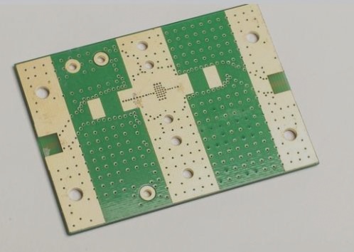
Common PCB Design Mistakes to Avoid
A Printed Circuit Board (PCB) is a vital component in electronic devices, serving as the foundation for the entire product. Avoiding common design mistakes is crucial for a successful PCB layout. Here are some key errors to watch out for:
1. Random Placement of Text
- Placing text on SMD soldering pads incorrectly can complicate testing and soldering.
- Text size matters – too small makes printing difficult, while too large can overlap and be hard to read.
2. Misuse of the Graphics Layer
- Unnecessary connections on graphics layers can lead to confusion and misunderstandings.
- Deviation from conventional design practices can create difficulties in the layout.
3. Overlapping Pads
Overlapping pads can lead to drilling issues and scrap during the manufacturing process.
4. Setting of Single-Sided Pad Aperture
- Single-sided pads should not be drilled, or if necessary, set the hole diameter to zero.
- Clearly mark single-sided pads for drilling to avoid issues.
5. Using Filler Blocks to Draw Pads
While filler blocks can pass design rule checks, they may not be ideal for processing, affecting solder mask application.
6. Electrical Ground Layer as a Flower Pad and Connection
Designing the power supply as a flower pad can lead to isolated connections if not done correctly.
7. Undefined Processing Levels
Specifying the processing order for multi-layer boards is essential to avoid soldering challenges.
8. Excessive or Thin Filler Blocks in PCB Design
Be cautious of filler block design to prevent data loss and complicated processing.
9. Surface Mount Device Pad Too Short
Short pads on surface mount devices can complicate continuity testing.
10. Small Spacing of Large-Area Grids
Maintain a minimum spacing between lines to prevent manufacturing issues.
11. Distance Between Large-Area Copper Foil and Outer Frame Too Close
Ensure an adequate distance to prevent warping during manufacturing.
12. Short Shaped Holes
When designing a PCB, attention to detail and adherence to best practices can prevent costly mistakes and ensure a smooth manufacturing process.
Important Considerations for PCB Design
- Aspect Ratio for Shaped Holes: The length-to-width ratio of shaped holes should be at least 2:1, with a width greater than 1.0mm. Smaller dimensions may lead to drilling issues, as well as increased processing difficulties and costs.
- Uneven Graphic Design: Discrepancies in plating layers during pattern plating can have a negative impact on the overall quality of the PCB.
- Unclear PCB Outline Frame Design: Inconsistencies in contour lines for layers such as Keep, Board, Top over, etc., can pose challenges for PCB manufacturers, making it difficult for them to determine the correct contour line to follow.
Latest Updates:
Recent advancements in PCB technology have introduced innovative solutions to address these common design issues. For instance, the development of advanced drilling techniques has helped improve the precision and efficiency of hole shaping processes, reducing the likelihood of drilling-related problems.
Additionally, manufacturers are now utilizing sophisticated software tools to ensure precise alignment of plating layers during pattern plating, enhancing the overall quality and reliability of PCBs.
Furthermore, the use of automated design verification systems has significantly improved the accuracy of PCB outline frame designs, minimizing errors and streamlining the manufacturing process.