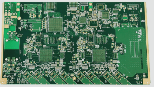
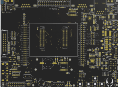
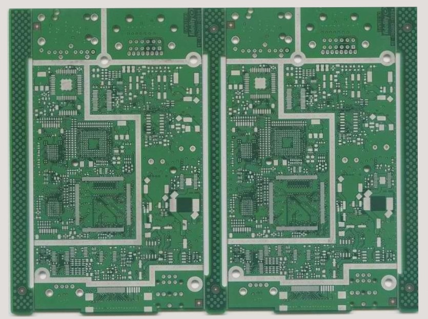
Essential Circuit Board Design Skills for Engineers
For seasoned engineers, PCB board design is a smooth process, with attention to detail and operational skills finely tuned over time. However, for newcomers in the field, mastering circuit board design can pose challenges. Lack of proficiency may lead to potential design issues, emphasizing the need for a thorough understanding of circuit board design.

Key Circuit Board Design Skills:
- Skill 1: Clear Definition of Processing Level
- Tip 2: Maintain Distance Between Copper Foil and Outer Frame
- Tip 3: Avoid Using Padding for Pads
- Tip 4: Separate Electrical Ground from Pads and Wires
- Tip 5: Ensure Adequate Pad Length
- Tip 6: Avoid Pad Overlaps
Ensure clarity in the file to reduce plate-making errors. Pay special attention to instructions for single-sided circuit boards to avoid welding issues.
Keep a minimum distance of 0.2mm between large-area copper foil and the outer frame to prevent solder resist peeling off.
Do not draw pads using filler blocks as it can complicate soldering during processing.
Avoid mixing the electrical ground layer with pads and connections to prevent power supply short circuits.
Prevent test pin misplacement by maintaining sufficient pad length for surface mount components.
Prevent scrap during the drilling process by ensuring pads do not overlap.
These six circuit board design skills are crucial for successful PCB design. While not overly complex, mastering these techniques significantly impacts design outcomes. Attention to these details is essential for achieving perfection in PCB board design.
For more information on PCB fabrication, visit Well Circuits.