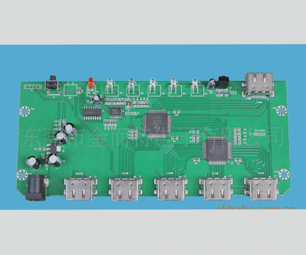
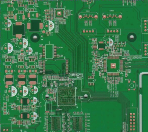
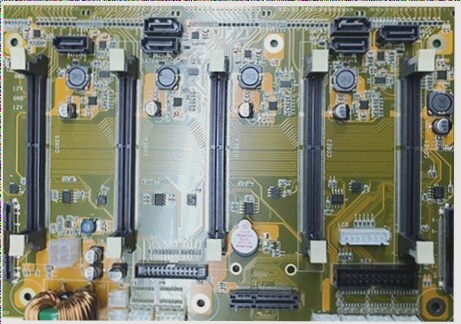
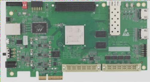
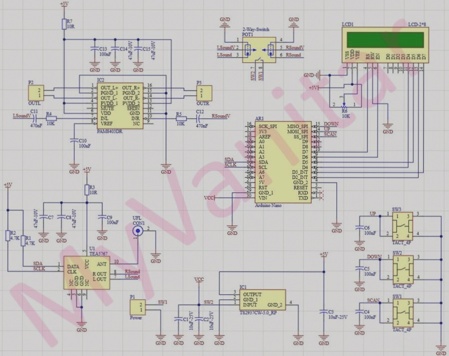
1. The PCBA processing procedure involves generating process and coordination files based on the Gerber files and BOMs provided by the customer.
2. After creating a plan, we prepare the necessary materials and ensure that everything is in order before commencing the production according to specifications.
3. It is essential for staff to wear anti-static gloves, and PCBA substrates must be organized properly; bare boards should not be stacked directly.
4. Next, I will delve into the PCBA processing steps and outline the key precautions to consider.
1. PCBA Processing Flow
1. PCBA Processing Technology: Based on the customer’s Gerber file and BOM list, we create the process file for SMT production and generate the SMT coordinate file.
2. Verify that all production materials are ready, compile complete orders, and confirm the PMC production plan.
3. Execute SMT programming and produce the first board for verification to ensure accuracy.
4. PCBA processing technology employs SMT methods to create laser-cut steel meshes.
5. Solder paste printing is utilized to guarantee that the printed solder paste is uniform, of appropriate thickness, and consistent.
6. Use the SMT placement machine to mount components onto the circuit board, performing online AOI automatic optical inspection as needed.
7. Establish an optimal reflow soldering furnace temperature curve, allowing the circuit board to undergo reflow soldering, transforming the solder paste from a paste and liquid state to a solid state for effective soldering after cooling.
8. PCBA processing technology has undergone the required IPQC inspection.
9. The DIP plug-in process involves passing the plug-in materials through the circuit board, which subsequently goes through wave soldering for connections.
10. Perform necessary post-furnace processes, including trimming leads, post-welding inspections, and cleaning the board surface.
11. QA conducts comprehensive testing to ensure quality in the PCBA processing technology.
2. PCBA Processing Precautions
1. Warehouse personnel must wear anti-static gloves when distributing materials and conducting IQC testing, reliably grounding with a meter; the work surface should be covered with anti-static rubber pads beforehand.
2. During operations, utilize an anti-static work surface and store components and semi-finished products in anti-static containers. Ensure welding equipment is grounded, and electric soldering irons must be anti-static, with all equipment tested prior to use.
3. When PCBA passes through the furnace, the pins of the plug-in components may be affected by the tin flow, leading to misalignment; therefore, repair personnel are required to make appropriate corrections after the soldering process.
4. While soldering PCBA for speakers and batteries, be cautious not to use excessive solder, which can cause short circuits or detachment of surrounding components.
5. PCBA substrates must be organized neatly; bare boards should not be stacked directly, and electrostatic bags must be utilized for stacking.