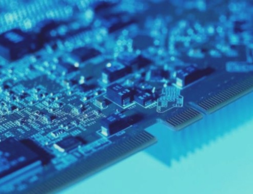
PCB Cloning Services: Revolutionizing Electronic Device Manufacturing
As technology continues to evolve rapidly, inefficiency and waste in electronic device manufacturing have become significant concerns. PCB clone services offer a solution to these challenges by providing efficient PCB replication. PCB cloning is crucial for replacing outdated PCBs that are no longer in production, especially in high-end applications where new PCB installation is a major challenge.
PCB fabrication has seen a surge in demand due to recent advancements in electrical appliance production. To meet the needs of electrical designers, creating new sets of PCBs through cloning has become essential.
Understanding PCB Cloning
PCB cloning, also known as PCB duplication or PCB copy, is a reverse engineering technique used to replicate existing PCB boards. By creating an exact replica of the original circuit board, PCB clones aim to copy and replace outdated circuit boards effectively.
The process of PCB cloning involves creating a Bill of Material (BOM) and duplicating schematics, essential steps in developing high-quality electronic devices. It allows for cost-effective redesign and modification of original designs to meet specific requirements.
Advantages of PCB Cloning
- The feasibility and premium quality of PCB clones make them a valuable asset in electronic device manufacturing.
PCB board fabrication is a time-consuming and complex process that requires high-quality materials. PCB manufacturers face significant challenges in meeting the demands of modern electronic devices, making PCB cloning a cost-effective solution for extending the life of devices and systems.
Benefits of PCB Cloning for Manufacturers
Creating PCB boards from scratch is a complex process compared to duplicating them. The initial costs of developing and testing prototypes, adjusting design parameters, and optimizing the design can be significant. However, PCB cloning offers a cost-effective alternative. By choosing PCB replication, you can avoid design costs and benefit from the advantages of reverse engineering techniques.
- Streamline Manufacturing: PCB cloning simplifies the process for manufacturers, allowing them to identify and replicate excellent designs effortlessly. This streamlines production activities, automates manufacturing techniques, reduces manual labor, and enhances product quality.
- Technique for Compassionate Engineering: Attention to detail is crucial when relying on PCB clones. Engineers can create high-quality products tailored to meet specific needs and perform reliably under various conditions. Debugging limitations on existing designs drive engineers to enhance product performance continually.
- Increased Scalability and Independence: PCB clones offer companies flexibility during manufacturing, enabling them to produce a large number of boards from a single design. This scalability helps meet consumer demands, improve production processes, align manufacturing operations with customer designs, and increase revenue.
- Consistent Performance: Mass-producing PCB boards using clones ensures uniformity in design and performance across all boards. The consistent performance of these boards, especially in high-speed applications, outperforms traditional PCBs due to their unique properties.
When receiving a PCB for cloning, documenting component types, specifications, locations, and taking digital photos are essential steps. Cleaning the PCB thoroughly, scanning it accurately, and utilizing software like Photoshop at the right resolution are critical for successful replication.

Steps to Create a PCB Design:
- Begin by polishing the top thin coating and bottom coat lightly with water yarn paper until the copper film shines. Scan the PCB, open Photoshop, and swap the colors of the two layers.
- Create a new PCB component editor. Select a component from the PORTEL99 editor and paste it into the component editor.
- After finalizing the component packages, open them in the PROTEL 99 editor and save them as a CAD file.
- Open both the CAD and imported CAD files in the PCB image. Copy the component package to the CAD alongside the PCB image.
- Focus on the SILK layer on the PCB (the yellow layer), trace the line in the TOP layer, and implement the device following the instructions in step 2. Once done, remove the SILK layer. Opting for PCB duplication can save design costs.
- There are two types of circuit boards: PCB and BOT. Convert the PCB to PROTEL and merge the two schematics into one.
- Print the TOP LAYER and BOTTOM LAYER (1:1 ratio) on transparent film using a laser printer. Place the film on the PCB, check for errors, and proceed.
Conclusion:
The field of electronics is rapidly evolving in today’s world. It stands out for its openness to new concepts. The importance of PCB clones cannot be overstated. When market innovations arise, electronic manufacturers constantly seek to tweak their PCB designs.