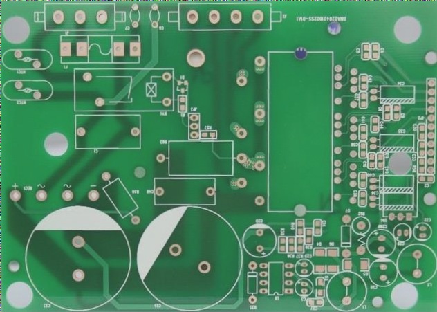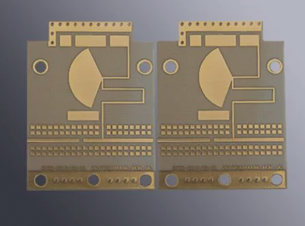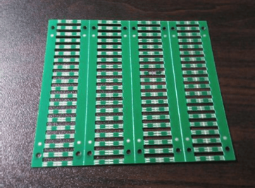
**Pad Aperture and Pad Width**
1. According to the processing capabilities of mainstream PCB manufacturers, the aperture of pads should not be less than 0.2mm if drilled mechanically, and 4mil if drilled by laser. The aperture tolerance may vary slightly depending on the board type, but it is generally controllable within 0.05mm. Pad width should not be less than 0.2mm.
**The Spacing Between Pads**
2. Based on the processing capabilities of mainstream PCB manufacturers, the spacing between pads should not be less than 0.2mm.
**The Spacing Between Copper Skin and the Edge of the Plate**
3. The distance between charged copper skin and the edge of the PCB board should not be less than 0.3mm. This spacing rule should be set on the Design Rules – Board Outline page, as shown in the figure above.
4. For large areas of copper, a shrinkage distance from the board edge is usually required, typically set to 20mil. In the PCB design and manufacturing industry, engineers often leave a 20mil margin from the edge of the board to prevent issues like coiling or electrical short circuits caused by copper skin extending to the edge. To manage this indented copper skin, one approach is to draw a keepout layer on the edge of the board and set the distance between the copper and the keepout layer. A simple method is to set different safety distances for copper areas; for example, a safety distance of 10mil for the entire board and 20mil for copper areas. This achieves the effect of a 20mil edge shrinkage and removes potential dead copper in the device.
**Non-Electrical Safety Spacing:**
**Character Width, Height, and Spacing**
5. During processing, no changes can be made to the text film except that the line width of characters with a D-code less than 0.22mm (8.66mil) will be increased to 0.22mm. Thus, the character line width should be L0.22mm (8.66mil). The width of the entire character should be W1.0mm, the height should be H1.2mm, and the spacing between characters should be D0.2mm. If the text falls below these standards, it may appear blurred during printing.
**Through-Hole to Through-Hole Spacing (Hole Edge to Hole Edge)**
6. The spacing between through-holes (VIA) should be greater than 8mil.
**Distance from Screen to Pad**
7. Screen printing should not overlap with pads. If silk screen covers the pads, solder will not adhere properly, affecting component installation. Generally, an 8mil spacing is recommended. If the PCB board is densely packed in a limited area, a 4mil spacing may be acceptable. If screen printing accidentally covers a pad during design, the board manufacturer will automatically remove the screen print from the pad during production to ensure proper soldering.
8. However, in specific cases, the screen might be intentionally close to the pad to prevent solder connections from short-circuiting during soldering, particularly when pads are very close together. This scenario requires a different approach.
**3D Height and Horizontal Spacing on Mechanical Structures**
9. PCB components should be installed horizontally with adequate height and spacing to avoid conflicts with other mechanical structures. Therefore, the design must consider the spatial structure between components and between the PCB and the product enclosure, ensuring safe spacing for all components to prevent spatial conflicts.
**How to Solve the Problem of Insufficient Spacing?**
10. Since spacing is measured in the air (line of sight), proper layout can help reduce the required spacing. Insulation and bilateral assembly can significantly reduce spacing requirements. Insulation might involve barriers between high-voltage nodes. Components mounted on the surface allow circuits needing spacing to be placed on opposite sides of the board. High-voltage circuits should generally be placed on the top of the board, with low-voltage circuits on the bottom for control and monitoring, as low-voltage circuits do not have the same creepage requirements as high-voltage circuits.
**How to Solve the Problem of Insufficient Creepage Distance?**
11. Creepage distance refers to the distance between electrical nodes on an insulating surface, meaning the space between conductors on the surface or inner layers of the PCB. However, component expansion is constrained by the product’s volume, so alternative strategies are needed to meet creepage distance requirements while accommodating higher package density.
**Standard for Calculating Conductor Spacing at Various Voltage Levels**
12. Maintaining proper distance between PCB wires is crucial to prevent short circuits. There is no one-size-fits-all solution, as different industrial and safety standards specify varying spacing requirements based on voltage, application, and other factors. Considerations include:
13. For products undergoing safety certification, each facility has specific standards for insulation requirements. For example, in the United States, PCB spacing for most mains or battery-powered information technology equipment should be determined according to tables 2K, 2L, 2M, or 2N of the UL IEC60950-1 standard, Edition 2. These tables specify safe distances and “creepage distances” for different insulation classes.
14. The required spacing depends on the circuit’s location. When evaluating spacing and creepage requirements, consider pollution levels and insulation types. Pollution levels refer to the amount of dust, moisture, and other particulate matter between high-voltage nodes. The standard includes various insulation types: functional, basic, complementary, double, and reinforced. Creepage distance standards also vary by insulation class. The following figure illustrates the creepage distance required by IEC60950-1 for different voltage levels. For double or reinforced insulation classes, the data should be doubled.


