Precautions for Selective Wave Soldering Carrier and Circuit Board Design:
- Ensure solder pins of traditional plug-ins are not too close to the edge of the carrier to avoid solder insufficiency due to the shadow effect.
- Effectively cover areas not requiring soldering with the tin furnace using the carrier.
- Maintain a minimum wall thickness of 0.05” (1.27mm) at the edge of carrier holes to prevent unintended solder penetration.
- Keep components needing tin furnace soldering at least 0.1” (2.54mm) away from the edge of carrier holes to minimize shadow effects.
- Components passing through the furnace surface should have a height less than 0.15” (3.8mm) to ensure proper coverage by the furnace carrier.
- Choose a soldering furnace carrier material that does not react with solder, withstands high temperatures without deforming, is heat-resistant, lightweight, and minimally shrinks when heated. Common materials include aluminum alloy and synthetic stone.
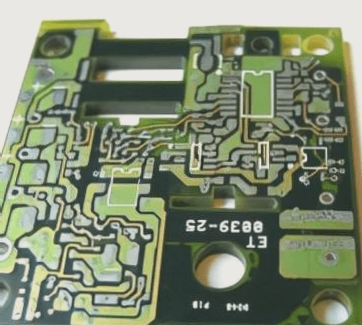
- Initially, PCB boards were designed with traditional insertion methods and required wave soldering. Subsequently, Surface Mount Technology (SMT) processing was introduced.
- Mixed use of PCBA patch processing and wave soldering became common with the advancement of processing technology, especially for components that couldn’t be converted to SMT.
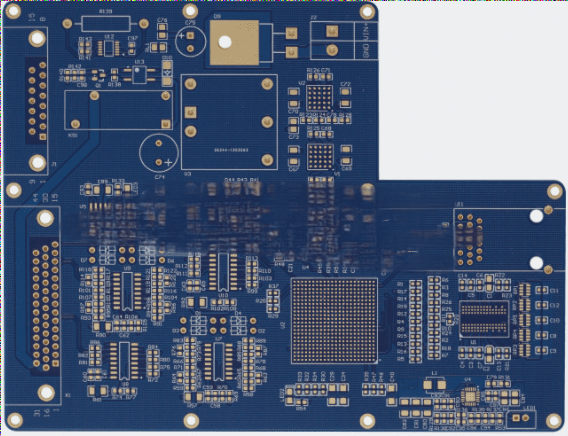
- Arrange all plug-in components on one side of the board and designate the opposite side for wave soldering during board design. Secure PCBA patch processing components on the wave soldering side with red glue to prevent them from falling into the tin furnace.
- Modern boards mostly undergo dual-side PCB processing, with selective wave soldering emerging to address components that can’t be fully processed using PCBA patch processing.
For more information on PCB fabrication and PCBA assembly, feel free to explore our website!