There is a common saying: “Details determine success or failure.” The gap between a novice PCB engineer and an experienced veteran often lies in the finer points.
1. Be mindful of the placement orientation and distance of components at the edges of the PCB.
Since PCBs are typically manufactured using a jigsaw method, devices positioned near the edge must adhere to two key criteria.
First, they should be aligned parallel to the cutting direction to ensure uniform mechanical stress on the device. For instance, if the component is oriented like the one shown on the left side of the figure above, the differing force directions on the two pads of the component may lead to separation or detachment during soldering.
Second, components must be spaced beyond a certain threshold to avoid damage during the cutting process.
2. Pay attention to the spacing between components.
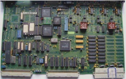
The spacing between SMD components is a crucial consideration for engineers during layout. If the spacing is too tight, it becomes challenging to print solder paste effectively, leading to issues with soldering and tinning.
**Distance recommendations are as follows:**
1. **Device distance requirements between patches:**
– Same type of devices: ≥0.3mm
– Dissimilar devices: ≥0.13*h + 0.3mm (where h is the maximum height difference between neighboring components)
2. **The distance between components requiring manual placement:**
– ≥1.5mm
These recommendations are for reference only and should be aligned with the PCB design specifications of individual companies.
3. **Consider the distance between wires or components and the edge of the board:**
– Leads or components should not be placed too close to the edge of the board, particularly on single-sided boards. Single-sided boards are often made of paper materials, which are prone to breaking under stress. Connecting or placing components at the edge can lead to damage.
4. **Placement of decoupling capacitors for ICs:**
– A decoupling capacitor should be positioned near the power port of each IC, ideally as close as possible to the port. For chips with multiple power ports, a decoupling capacitor should be placed at each one.
5. **Treatment of line corners:**
– Typically, wire thickness changes at corners, causing reflections. The corner method can exacerbate thickness changes; a 45-degree angle is preferable, while rounded corners offer the best results. However, rounded corners can complicate PCB design, so their use should be determined by signal sensitivity. For standard signals, a 45-degree angle is generally adequate, with rounded corners reserved for highly sensitive lines.
6. **Avoid placing via holes on pads:**
– It is advisable not to drill through holes on pads, as this can easily result in solder leaks.
7. **Ensure lead widths on both sides of the component pad are identical:**
– The lead width on either side of the component pad should match.
8. **Add teardrops if the lead is smaller than the plug-in pad:**
– If the wire diameter is smaller than the pad of the through-hole device, teardrops should be added.
The inclusion of teardrops offers several advantages:
1. They prevent abrupt decreases in signal line width, reducing reflection and ensuring a smoother transition between the trace and the component pad.
2. They address the issue of the connection between the pad and trace being easily damaged by impact.
3. Teardrops enhance the overall aesthetic of the PCB.
1. Be mindful of the placement orientation and distance of components at the edges of the PCB.
Since PCBs are typically manufactured using a jigsaw method, devices positioned near the edge must adhere to two key criteria.
First, they should be aligned parallel to the cutting direction to ensure uniform mechanical stress on the device. For instance, if the component is oriented like the one shown on the left side of the figure above, the differing force directions on the two pads of the component may lead to separation or detachment during soldering.
Second, components must be spaced beyond a certain threshold to avoid damage during the cutting process.
2. Pay attention to the spacing between components.

The spacing between SMD components is a crucial consideration for engineers during layout. If the spacing is too tight, it becomes challenging to print solder paste effectively, leading to issues with soldering and tinning.
**Distance recommendations are as follows:**
1. **Device distance requirements between patches:**
– Same type of devices: ≥0.3mm
– Dissimilar devices: ≥0.13*h + 0.3mm (where h is the maximum height difference between neighboring components)
2. **The distance between components requiring manual placement:**
– ≥1.5mm
These recommendations are for reference only and should be aligned with the PCB design specifications of individual companies.
3. **Consider the distance between wires or components and the edge of the board:**
– Leads or components should not be placed too close to the edge of the board, particularly on single-sided boards. Single-sided boards are often made of paper materials, which are prone to breaking under stress. Connecting or placing components at the edge can lead to damage.
4. **Placement of decoupling capacitors for ICs:**
– A decoupling capacitor should be positioned near the power port of each IC, ideally as close as possible to the port. For chips with multiple power ports, a decoupling capacitor should be placed at each one.
5. **Treatment of line corners:**
– Typically, wire thickness changes at corners, causing reflections. The corner method can exacerbate thickness changes; a 45-degree angle is preferable, while rounded corners offer the best results. However, rounded corners can complicate PCB design, so their use should be determined by signal sensitivity. For standard signals, a 45-degree angle is generally adequate, with rounded corners reserved for highly sensitive lines.
6. **Avoid placing via holes on pads:**
– It is advisable not to drill through holes on pads, as this can easily result in solder leaks.
7. **Ensure lead widths on both sides of the component pad are identical:**
– The lead width on either side of the component pad should match.
8. **Add teardrops if the lead is smaller than the plug-in pad:**
– If the wire diameter is smaller than the pad of the through-hole device, teardrops should be added.
The inclusion of teardrops offers several advantages:
1. They prevent abrupt decreases in signal line width, reducing reflection and ensuring a smoother transition between the trace and the component pad.
2. They address the issue of the connection between the pad and trace being easily damaged by impact.
3. Teardrops enhance the overall aesthetic of the PCB.

 العربية
 简体中文
简体中文 Nederlands
 English
 Français
 Deutsch
 Italiano
 日本語
日本語 한국어
한국어 Português
 Русский
 Español
 ไทย
ไทย