Understanding Printed Circuit Boards (PCBs)
A printed circuit board, also known as a PCB, is a vital component in electronic devices. It serves as an insulation board with a conductive pattern and holes to connect electronic parts. PCBs are essential for supporting electronic components and ensuring proper electrical connections.
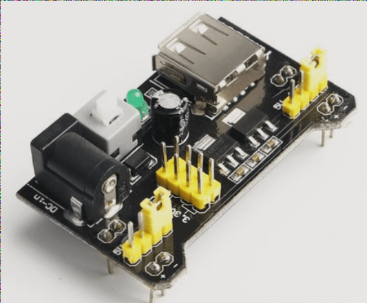
PCBs come in various colors for component legends, with white being common for boards with green, blue, or red masks, and black for white or yellow masks. Custom colors are also available based on client preferences.
Optimizing PCB Manufacturing
To reduce costs in PCB manufacturing, it’s important to evaluate the necessity of component legends on both sides of the board. Sometimes, having legends only on the component side can be sufficient, especially for boards with minimal components. This evaluation can lead to cost savings and streamlined production processes.
Streamlining PCB Design
Many PCBs feature minimal information on the solder side, which may not be essential. Including unnecessary details can increase costs and production time. Simplifying the design by removing non-essential elements can improve efficiency and reduce expenses.
The Role of PCBs in Electronics
PCBs play a crucial role in electronic device manufacturing by eliminating errors in wiring and ensuring consistent assembly of components. They contribute to the quality and reliability of electronic devices, enhancing productivity and cost-effectiveness in production processes.
Evolution of Printed Circuit Boards
Printed circuit boards have evolved from single-layer to multi-layer and flexible designs. The trend towards high accuracy, density, and reliability in PCB development has led to enhanced electronic device performance and cost savings. Future PCB manufacturing technologies are expected to focus on high precision, small size, and improved efficiency.
Historical Significance of PCBs
Printed circuit boards have a rich history, dating back to the 1930s when they were first used in radio technology. Since their commercial adoption in the late 1940s, PCBs have revolutionized the electronics industry. Today, they are integral to electronic component connections and have become indispensable in electronic device manufacturing.
Components of a PCB
PCBs consist of various elements such as pads, through holes, mounting holes, wires, connectors, and electrical boundaries. These components serve specific functions in ensuring proper connectivity and functionality within the circuit board.
PCB Components Overview
- Wiring: The process of connecting component pins with electrical copper foil.
- Connector: Used for linking components to a PCB.
- Charger: Aids in reducing impedance control by enhancing the copper cladding of the earth grid.
- Electrical Limit: Ensures that the size of the PCB and its components stay within specified boundaries.

Advantages of PCBs
PCBs offer various benefits that make them highly preferred in electronics:
- High Density: Evolution in integrated circuit integration and assembly techniques has led to high-density PCBs.
- High Reliability: PCBs undergo thorough testing to ensure long-lasting performance.
- Determinability: Standardized PCB properties streamline design processes, saving time and enhancing production efficiency.
- Manufacturability: Standardization, sizing, and automation in production ensure consistent quality.
- Testability: Rigorous testing procedures are in place to assess PCB yield and longevity.
- Mountability: PCBs are easy to connect and automate in manufacturing, facilitating component mounting.
- Sustainability: Standardized components and efficient design allow for easy system modifications and repairs.
The Green Color of PCBs
Ever wondered why printed circuit boards are predominantly green in color? Here’s why:
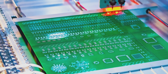
The green solder mask used on PCBs serves to shield electronic traces from moisture and dust while regulating solder flow. While PCBs can come in various colors like yellow, blue, red, and black, green remains popular for a few reasons:
- Cost-Effective: Green solder masks are cheaper to produce compared to other colors.
- Manufacturing Processes: Green facilitates optical positioning calibration during PCB manufacturing and assembly processes.
- Worker Comfort: Green is easier on the eyes for workers visually inspecting PCBs, especially under harsh lighting conditions.


