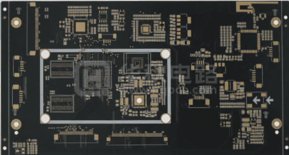
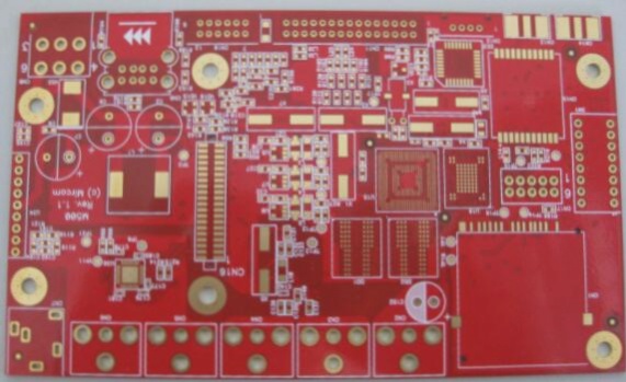
The six-layer PCB consists of six conductive layers, including a four-layer PCB with two planes situated between additional signal layers. A typical six-layer PCB features two inner layers, two outer layers, and two planes—one dedicated to power and the other to ground. This configuration enhances electromagnetic interference (EMI suppression) and provides improved routing options for both low-speed and high-speed signals. The two outer layers assist with low-speed signal transmission, while the inner layers support high-speed signals.
The proper stacking of a six-layer PCB can significantly enhance its performance. Due to the use of various types of radio frequency equipment, this design effectively suppresses EMI and accommodates multiple spacing components. Any design errors may compromise the PCB’s optimal performance. Therefore, how should we approach the design to fully leverage the PCB’s capabilities?
First, before starting the design process, it is essential to assess and determine the number of grounding, power, and signal planes required for the PCB. Bonding layers play a crucial role in the laminate structure as they provide improved shielding and reduce the need for external shielding enclosures.

**If you are planning to design a compact circuit board with limited space for routing, you can use a stack of four signal layers, a ground layer, and a power layer.**
In high-density circuit boards, a combination of wireless and analog signals is often used. The signal layer/ground/power layer/ground/signal layer/ground layer stacking method separates the inner and outer signal layers, creating a configuration with both internal and external signals. This layered arrangement helps mitigate electromagnetic interference (EMI) within the internal signal layers. Stacked designs are particularly beneficial for RF applications, as the AC power and ground planes provide excellent decoupling.
**Dense PCBs**
For printed circuit boards (PCBs) with many sensitive circuits, the optimal stack is signal/power/2 signal/ground/signal. This stack effectively shields sensitive traces and is better suited for high-frequency analog or high-speed digital circuits. It keeps these signals separated from the slower signals on the outer layers. The shielding occurs on the inner layers, allowing routing of signals with varying frequencies or switching speeds.
**A printed circuit board**
The ground/signal/power/ground/signal/ground stack is ideal for placement near sources of strong radiation. This configuration effectively suppresses electromagnetic interference and is well-suited for circuits used in noisy environments.
Since the six-layer PCB design has become a standard feature in many advanced electronic circuits and is widely used by electronic manufacturers, what are its key advantages?
**Six-layer PCB Design**
Thanks to their multi-layer design, six-layer PCBs are more compact than traditional circuit boards, which is especially beneficial for miniature devices. The design of the six-layer stack requires careful planning, which minimizes the potential for errors and ensures high-quality construction. Currently, various testing and inspection methods are employed to confirm the reliability of the circuit board.
The compactness of a six-layer PCB is achieved by using lightweight components, which helps reduce the overall weight of the board. Unlike single-layer or double-layer PCBs, six-layer designs allow for interconnection of components without the need for multiple connectors.
A six-layer PCB consists of several insulating layers created by bonding protective materials and prepregs, enhancing the durability of the board.
With excellent electrical performance and a compact design, six-layer PCBs can efficiently support high-speed, high-capacity applications.
If you have any PCB manufacturing needs, please do not hesitate to contact me.Contact me
The proper stacking of a six-layer PCB can significantly enhance its performance. Due to the use of various types of radio frequency equipment, this design effectively suppresses EMI and accommodates multiple spacing components. Any design errors may compromise the PCB’s optimal performance. Therefore, how should we approach the design to fully leverage the PCB’s capabilities?
First, before starting the design process, it is essential to assess and determine the number of grounding, power, and signal planes required for the PCB. Bonding layers play a crucial role in the laminate structure as they provide improved shielding and reduce the need for external shielding enclosures.

**If you are planning to design a compact circuit board with limited space for routing, you can use a stack of four signal layers, a ground layer, and a power layer.**
In high-density circuit boards, a combination of wireless and analog signals is often used. The signal layer/ground/power layer/ground/signal layer/ground layer stacking method separates the inner and outer signal layers, creating a configuration with both internal and external signals. This layered arrangement helps mitigate electromagnetic interference (EMI) within the internal signal layers. Stacked designs are particularly beneficial for RF applications, as the AC power and ground planes provide excellent decoupling.
**Dense PCBs**
For printed circuit boards (PCBs) with many sensitive circuits, the optimal stack is signal/power/2 signal/ground/signal. This stack effectively shields sensitive traces and is better suited for high-frequency analog or high-speed digital circuits. It keeps these signals separated from the slower signals on the outer layers. The shielding occurs on the inner layers, allowing routing of signals with varying frequencies or switching speeds.
**A printed circuit board**
The ground/signal/power/ground/signal/ground stack is ideal for placement near sources of strong radiation. This configuration effectively suppresses electromagnetic interference and is well-suited for circuits used in noisy environments.
Since the six-layer PCB design has become a standard feature in many advanced electronic circuits and is widely used by electronic manufacturers, what are its key advantages?
**Six-layer PCB Design**
Thanks to their multi-layer design, six-layer PCBs are more compact than traditional circuit boards, which is especially beneficial for miniature devices. The design of the six-layer stack requires careful planning, which minimizes the potential for errors and ensures high-quality construction. Currently, various testing and inspection methods are employed to confirm the reliability of the circuit board.
The compactness of a six-layer PCB is achieved by using lightweight components, which helps reduce the overall weight of the board. Unlike single-layer or double-layer PCBs, six-layer designs allow for interconnection of components without the need for multiple connectors.
A six-layer PCB consists of several insulating layers created by bonding protective materials and prepregs, enhancing the durability of the board.
With excellent electrical performance and a compact design, six-layer PCBs can efficiently support high-speed, high-capacity applications.
If you have any PCB manufacturing needs, please do not hesitate to contact me.Contact me


