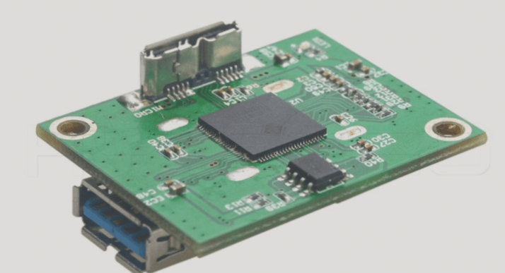
High-Density PCB Circuit Boards: Meeting Modern Electronic Component Challenges
Traditional PCB design encompasses single-sided, double-sided, and multi-layer boards, with multi-layer boards further categorized into single-press and multi-press geometric structures. However, current geometric structures often fall short in meeting the mounting density and electrical performance demands of contemporary electronic components.
To address these challenges, innovative approaches are being explored:
- Enhancing component connection density by reducing circuit and connection point spacing, enabling more contacts within a compact area.
- Exploring the stacking of different components in the same location to increase structural density.
High-density circuit boards pose not only technical challenges but also significant considerations in electronic assembly and construction. The demand for high-density technology is evident in various 3C products.
Benefits of High-Density PCB Circuit Boards
Adopting a high-density PCB circuit board design offers numerous advantages for electronic products:
- Reduction in the number of layers, leading to the creation of traditional and complex structures while lowering product costs.
- Increased line density through microvia technology, concealing wiring for interconnections and supporting advanced packaging technologies.
- Minimized signal reflection and crosstalk interference, enhancing electrical performance and signal accuracy.
- Thinner dielectric layers with micro-holes for improved signal transmission reliability.
- Decreased radio frequency and electromagnetic wave interference by reducing the distance between ground and signal layers.
- Flexibility in circuit configuration and design with microporous technology.
Meeting the Demand for Mobility and Functionality
The push for high density in electronic products stems from the increasing functionality, integration, and demand for mobility, thinness, and multifunctionality. As consumer preferences shift towards lightweight, slim, and aesthetically pleasing electronic devices, the need for high-density PCB circuit boards becomes more pronounced.
New business behaviors and innovative approaches are emerging to align with trends for lightweight, slim designs while maintaining commercial viability at low unit prices. The evolution of electronic component carriers, such as PCB circuit boards, reflects a clear trend in mobile electronics.