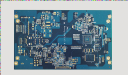
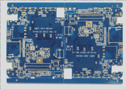
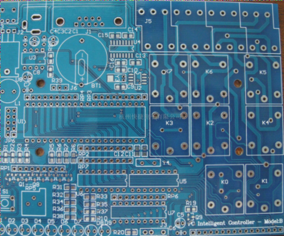
Copper Cladding in PCB Manufacturing: Enhancing Performance
Copper cladding is a crucial process in PCB manufacturing where non-wiring areas are covered with copper foil, improving ground plane quality, reducing loop area, minimizing voltage drop, and enhancing power efficiency and resistance to EMI. By lowering impedance and optimizing current loop area, copper cladding strengthens signal performance.
Key Steps in Copper Cladding
- Surface Preparation: Clean the PCB surface to enhance copper adhesion.
- Copper Foil Application: Attach copper foil to desired areas.
- Connection to Ground: Ensure proper grounding for efficiency.
- Etching: Remove excess copper to form the desired pattern.
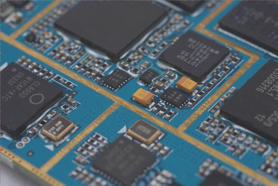
DPC Substrate and Copper Cladding
DPC substrates utilize direct-plated copper for efficient high-density designs, supporting finer lines and tighter tolerances critical for modern PCBs.
Comparison with Thick Film Process
While copper cladding enhances ground planes and signal integrity, the thick film process is ideal for robust, high-power circuits. Differences include the conductive material, application method, substrate, and main applications.
Conclusion
Copper cladding significantly boosts PCB performance by enhancing signal integrity and power distribution. Understanding the differences between copper cladding and the thick film process is crucial for optimal PCB design and production.
Copper and Alloy Materials in PCB Technology: A Comparative Analysis
Pure copper wire is known for its exceptional performance and stability over time, making it ideal for high-reliability applications. In contrast, silver-palladium alloys are susceptible to oxidation, migration, and lack long-term stability, impacting circuit reliability.
Bonding Strength in Metal-Ceramic PCB Manufacturing
The Significance of Strong Bonding Forces in Stone Ceramic Circuit Boards
- In the PCB industry, the bonding force between metals and ceramics typically ranges from 18 MPa to 30 MPa.
- Stone ceramic circuit boards demonstrate a remarkable bonding force of 45 MPa, ensuring high durability and stability.
- Strong bonding prevents detachment during use and maintains physical stability over time.
- Poor bonding force can lead to aging, deterioration, weaker adhesion, and potential failure.
Enhanced Precision and Stability in Stone Ceramic Circuit Boards
- The etching method in PCB manufacturing offers high precision with neat, burr-free edges and finely detailed lines.
- Stone ceramic circuit boards allow customization of copper thickness between 1μm and 1mm, with line widths and diameters as fine as 20μm.
- Printing methods result in rougher surfaces with less precision compared to etching, with copper thickness typically less than 20μm and minimum line width around 0.15mm.
Precision in Line Location and Surface Treatment
- Exposure and development methods offer high positioning accuracy for precise alignment of circuit patterns.
- Surface treatment techniques like nickel plating, gold plating, silver plating, and OSP enhance conductivity and durability.
- Various surface treatment methods have unique advantages, with silver-palladium alloy being a common material used.
Comparing LAM and DPC Processes in PCB Manufacturing
- LAM Process: Utilizes high-energy laser beams for precise bonding of ceramic and metal layers, offering customizable copper thickness and excellent graphic accuracy.
- DPC Process: Involves electroplating and sputtering techniques for metallizing ceramic surfaces, with a focus on copper seed layer deposition for circuit formation.
In conclusion, the selection of materials and processes in PCB manufacturing significantly impacts performance, reliability, and longevity. Strong bonding forces in ceramic circuits and precision in manufacturing processes are crucial for the durability and stability of modern electronic applications.