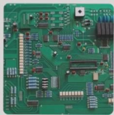
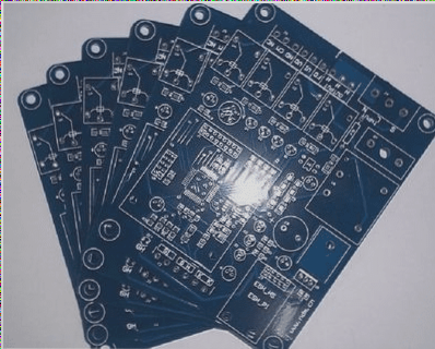
The Common Issues with Copper Foil in PCB Fabrication
- The copper foil used in PCB fabrication can be over-etched, leading to rejection in batch copper instances.
- Local collisions during the PCB process can cause separation of copper traces from the substrate, resulting in twisting or scratches on the traces.
- Using thick copper foils for designing thin circuits may cause over-etching and wastage of copper.
Reasons for Lamination Process Challenges
During the lamination process, ensuring full bonding between copper foil and prepreg is crucial. Contamination of prepreg or damage to the matte surface of the copper foil can lead to inadequate bonding strength, causing positional inaccuracies or detachment of copper traces.
Factors Affecting Laminate Raw Materials
- Defective electrolytic copper foil, resulting from poor galvanization or copper plating, can lead to inadequate peel strength and detachment of copper traces.
- Mismatched copper foils with resin systems like HTg sheets can cause insufficient peel strength of metal-clad laminate, increasing the risk of copper trace detachment.
Potential Causes of Pad Detachment During Soldering
- Single and double panels with large ground areas are prone to pad detachment due to rapid heat dissipation and high soldering temperatures.
- Repeated soldering at a point can weaken PCB pads.
- Excessive heat or pressure during soldering can easily detach PCB pads.