1. **The Concept of Solder Mask**
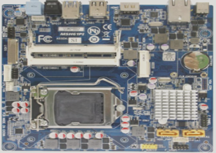
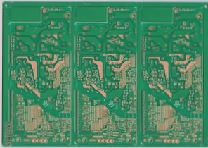
The solder mask refers to the layer of green epoxy applied to specific areas of the PCB (printed circuit board). This mask operates through a negative output process, meaning that when the solder mask is applied to the board, the areas not covered by the green epoxy expose the copper.
2. **Process Requirements for Solder Mask**
The solder mask plays a crucial role in minimizing solder defects during the reflow soldering process, and it is essential for PCB designers to minimize the spacing or air gaps surrounding pad features. While many process engineers prefer to separate all pad features with a solder mask, the pin spacing and pad size of fine-pitch components necessitate careful consideration. Although it may be acceptable for solder mask openings around QFPs (Quad Flat Packages) to remain unpartitioned on all four sides, managing solder bridges between component pins can become more challenging. For BGAs (Ball Grid Arrays), many companies offer solder masks that do not contact the pads but cover the areas between them to prevent solder bridging. Most surface mount PCBs are coated with a solder mask, but if the thickness exceeds 0.04 mm, it may adversely affect solder paste application. Surface mount PCBs, particularly those utilizing fine-pitch components, require a low-profile photosensitive solder mask.
3. **Process Production of Solder Mask**

Solder mask materials must be applied using either a liquid wet process or dry film lamination. Dry film solder mask materials are available in thicknesses ranging from 0.07 to 0.1 mm (0.03 to 0.04″), which can be suitable for certain surface mount products; however, this type is not advisable for close-pitch applications. While few companies offer thin enough dry film to meet standard fine-pitch requirements, several firms do provide liquid photosensitive solder mask materials. Typically, the solder mask opening should be 0.15 mm (0.006″) larger than the pad size, allowing for a 0.07 mm (0.003″) gap on all sides of the pad. Low-profile liquid photosensitive solder masks are cost-effective and are commonly used for surface mount applications, offering precise feature sizes and gaps.
**Understanding PCB Solder Mask Window Opening**
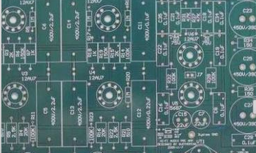
The solder mask opening denotes the area where copper is exposed at the points that require soldering—essentially, the dimensions of the area not covered by ink. The cover line indicates the dimensions of the circuit portions shielded by the solder mask. If the distance of the cover line is too small, it risks exposing the line during production.
**Reasons for Opening Windows in PCB Solder Mask**
1. **Aperture Opening**: Many customers prefer not to have ink obstruct small holes; without an opening, ink may seep into them. For larger holes, if filled with ink, customers may be unable to press keys properly. Additionally, for gold-plated components, it’s essential to open the window.
2. **PAD (Copper) Window Opening**: Customers require these openings for soldering and surface treatments (such as gold or tin plating).
If you have any PCB manufacturing needs, please do not hesitate to contact me.Contact me


