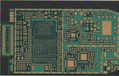
1. Using different resin systems and material substrates can lead to significant variations in the activation effect and copper plating quality, especially when copper treatment processes are involved.
2. Specifically, due to the unique properties of certain CEM composite substrates and high-frequency silver substrates, special treatment methods may be required for the chemical copper plating process. In some cases, standard chemical copper deposition may not yield satisfactory results.
3. Pretreatment of PCB substrates is crucial. Some substrates have a tendency to absorb moisture, and the resin-cured portion of pressure-formed substrates may be weak. As a result, during drilling, the resin may not provide sufficient strength, leading to poor drilling quality, increased hole count, or severe tearing of the hole wall resin. In such cases, baking the material beforehand may be necessary.
1. In addition, some multi-layer laminates may suffer from inadequate curing in the PP semi-cured substrate area, which directly impacts the drilling process and removal of rubber slag from active copper.
2. Poor drilling conditions are mainly reflected in: resin dust in the holes, rough hole walls, significant burrs, Konnemau thorns, nail-heads of inner copper foil, and uneven tear lengths in the glass fiber area. These issues can lead to hidden quality problems with chemical copper.
3. Apart from mechanically treating surface contamination and removing Konnemau thorns or burrs, the brush plate also helps clean the surface. In many cases, it plays an essential role in cleaning and removing dust from the holes.
4. In particular, the treatment of non-sticky slag in double-sided boards is crucial. It’s important to note that the presence of glue and dust does not automatically mean they will be removed with the slag. In fact, in many cases, the process of slag removal has limited impact on dust treatment. This is because the dust in the grooves can form small rubber clusters that make the grooves harder to clean. The rubber particles adsorbed on the hole walls may also detach during subsequent processing, potentially leading to the absence of copper in certain holes. Therefore, for multi-layer and double-sided boards, mechanical brushing and high-pressure cleaning are necessary, especially with the growing trend in the industry toward smaller hole sizes and higher aspect ratio plates. Ultrasonic cleaning is also becoming a trend to effectively remove dust from holes.
5. Proper and effective removal of adhesive slag can significantly improve hole adhesion and internal connectivity reliability. However, poor coordination between the PCB adhesive removal process and the groove treatment can result in various issues. Insufficient slag removal can cause quality problems such as micropores in the hole walls, poor inner layer bonding, hole wall shedding, and blow holes. On the other hand, excessive removal can lead to glass fibers protruding into the holes, rough hole walls, glass fiber cut-off points, copper leakage, or the destruction of the internal wedge-shaped hole, which compromises the separation of black copper in the inner layer. This may lead to broken or discontinuous copper in the holes, or stress-induced wrinkling of the copper coating.
6. Furthermore, coordinated control of the various groove fluids is crucial. Insufficient expansion or fluid flow may result in incomplete slag removal. However, expanding the fluids to an appropriate level helps remove fluffy resin, preventing defects like resin sinking or hole wall shedding in the post-processing stages. For glue tanks, using new grooves or achieving better handling activity may lead to improved results. However, excessive adhesive removal, particularly with single-functional, dual-functional, and some tri-functional resins, can lead to problems. Excessive removal can cause glass fibers to protrude from the hole walls, making it difficult to activate the fibers, reducing the bonding strength with chemical copper. As a result, the uniform deposition of chemical copper on the substrate will increase stress, and in the worst case, the chemical copper on the hole walls may peel off after the copper counterbore process. This can lead to a situation where there is no copper in subsequent holes, causing open circuits in the PCB. Such issues are not uncommon in the PCB industry, but the question remains: how can we control this effectively? Many have worked on solving this problem, but it persists and often repeats. Today’s production process might bring up new challenges, and tomorrow’s might present even more.