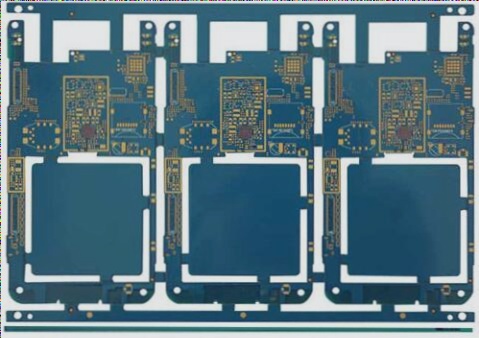
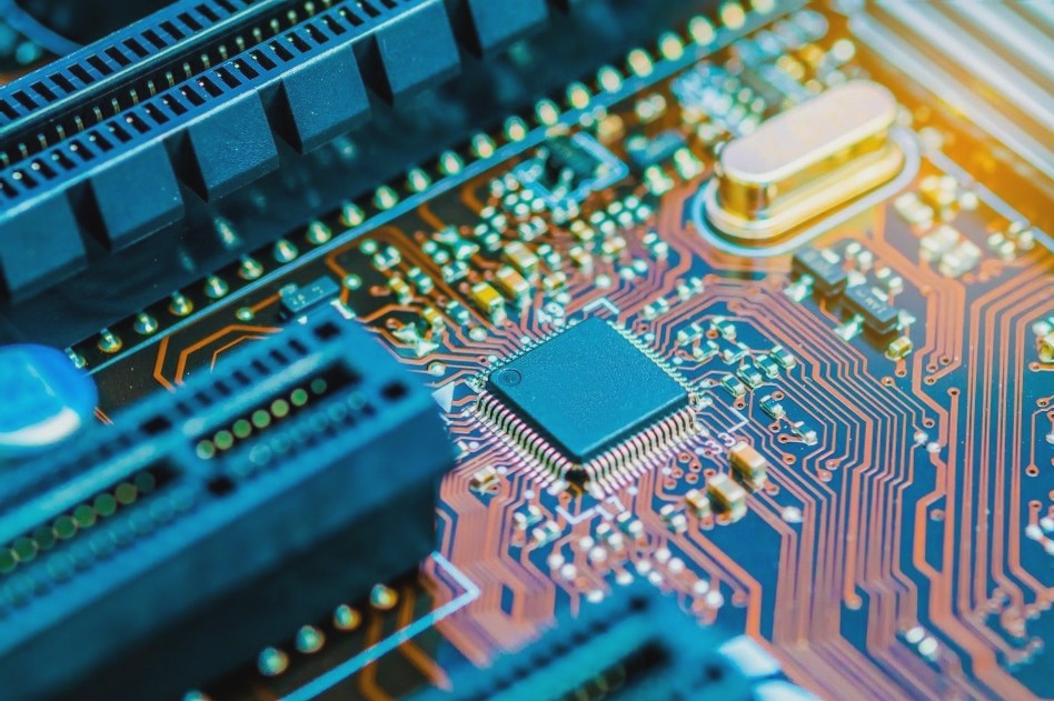
1. High-density interconnect (HDI) is one of the fastest-growing technologies in printed circuit board (PCB) design. Due to the more compact arrangement of smaller components, HDI boards allow for higher circuit density than traditional circuit boards, thereby creating more efficient pathways. Blind vias and/or buried vias are commonly used to optimize space on the HDI board, and microvias with diameters of 0.006 inches or less are increasingly employed.
2. Numerous vertical industries have incorporated HDI boards into their products, including manufacturers of military communications and strategic equipment, as well as medical diagnostic tools. The lightweight design of HDI boards also makes them ideal for aerospace applications, as well as smaller smartphones and laptops.

以下是对原文的逐行修改与润色:
—
The most common types of HDI boards include:
1. Through holes from surface to surface
2. A combination of through holes and buried holes
3. Multiple HDI layers incorporating through holes
4. Passive mounting base plates for non-electric installations
5. Coreless constructions using layer pairs
6. Replacement of coreless structures with layer pairs
**Benefits of HDI**
HDI boards are highly suitable and popular for a wide range of applications, including aviation, consumer electronics, computers, and other electronic products. Even in challenging environments, multilayer HDI boards offer enhanced reliability through the robust interconnection of stacked vias.
The reduction in component size provides designers with more workspace, thereby allowing design on both sides of the original PCB. Smaller components arranged together enable increased input and output capabilities, accelerating signal transmission and significantly reducing cross-delay and signal loss.
HDI technology enables the reduction of an eight-layer through-hole PCB to a four-layer HDI micro-hole PCB, achieving the same or improved functionality with fewer layers. This reduction substantially lowers material costs, making HDI technology highly cost-effective for electronics manufacturers. The superior performance of multi-layer HDI PCBs ensures reliability even in harsh environments.
**Why Use HDI?**
HDI boards, due to their lightweight, reliable performance, and compact size, are especially well-suited for wearable, mobile, and handheld electronic devices. These robust, smaller components, combined with high-density design geometries, enhance the functionality of PCBs and their final products.
With components placed closer together, the time required for electrical signals to propagate is reduced. The high-density design of HDI boards lowers signal rise time and inductance, minimizing the impact on adjacent pins and leads. The additional transistors not only support added functionality but also enhance overall performance.
Focusing on HDI design can reduce prototype development time and costs, shorten delivery timelines, and increase profit margins.
HDI technology results in products that are lighter, faster, and more efficient, while also enabling smaller packaging. The reduced size facilitates the design of compact end products that meet consumer demand for portability. While HDI design may involve a steep learning curve, the resulting benefits in productivity, reliability, and fewer manufacturing delays make the training worthwhile as market relevance grows.
2. Numerous vertical industries have incorporated HDI boards into their products, including manufacturers of military communications and strategic equipment, as well as medical diagnostic tools. The lightweight design of HDI boards also makes them ideal for aerospace applications, as well as smaller smartphones and laptops.

以下是对原文的逐行修改与润色:
—
The most common types of HDI boards include:
1. Through holes from surface to surface
2. A combination of through holes and buried holes
3. Multiple HDI layers incorporating through holes
4. Passive mounting base plates for non-electric installations
5. Coreless constructions using layer pairs
6. Replacement of coreless structures with layer pairs
**Benefits of HDI**
HDI boards are highly suitable and popular for a wide range of applications, including aviation, consumer electronics, computers, and other electronic products. Even in challenging environments, multilayer HDI boards offer enhanced reliability through the robust interconnection of stacked vias.
The reduction in component size provides designers with more workspace, thereby allowing design on both sides of the original PCB. Smaller components arranged together enable increased input and output capabilities, accelerating signal transmission and significantly reducing cross-delay and signal loss.
HDI technology enables the reduction of an eight-layer through-hole PCB to a four-layer HDI micro-hole PCB, achieving the same or improved functionality with fewer layers. This reduction substantially lowers material costs, making HDI technology highly cost-effective for electronics manufacturers. The superior performance of multi-layer HDI PCBs ensures reliability even in harsh environments.
**Why Use HDI?**
HDI boards, due to their lightweight, reliable performance, and compact size, are especially well-suited for wearable, mobile, and handheld electronic devices. These robust, smaller components, combined with high-density design geometries, enhance the functionality of PCBs and their final products.
With components placed closer together, the time required for electrical signals to propagate is reduced. The high-density design of HDI boards lowers signal rise time and inductance, minimizing the impact on adjacent pins and leads. The additional transistors not only support added functionality but also enhance overall performance.
Focusing on HDI design can reduce prototype development time and costs, shorten delivery timelines, and increase profit margins.
HDI technology results in products that are lighter, faster, and more efficient, while also enabling smaller packaging. The reduced size facilitates the design of compact end products that meet consumer demand for portability. While HDI design may involve a steep learning curve, the resulting benefits in productivity, reliability, and fewer manufacturing delays make the training worthwhile as market relevance grows.


